Datasheet 搜索 > 微控制器 > Cypress Semiconductor(赛普拉斯) > CY8C4125LQI-483T 数据手册 > CY8C4125LQI-483T 用户编程技术手册 1/43 页
 器件3D模型
¥ 0.471
CY8C4125LQI-483T 用户编程技术手册 - Cypress Semiconductor(赛普拉斯)
制造商:
Cypress Semiconductor(赛普拉斯)
分类:
微控制器
封装:
QFN-40
Pictures:
3D模型
符号图
焊盘图
引脚图
产品图
页面导航:
引脚图在P9P10P11P12Hot
原理图在P4
封装尺寸在P36P37P38
型号编码规则在P33P34
封装信息在P35
焊接温度在P35
功能描述在P1
技术参数、封装参数在P18P19P20P21P22P23P24P25P26P27P28P29
应用领域在P1
电气规格在P18

导航目录
CY8C4125LQI-483T数据手册
Page:
of 43 Go
若手册格式错乱,请下载阅览PDF原文件

PSoC
®
4: PSoC 4100 Family
Datasheet
Programmable System-on-Chip (PSoC
®
)
Cypress Semiconductor Corporation • 198 Champion Court • San Jose, CA 95134-1709 • 408-943-2600
Document Number: 001-87220 Rev. *E Revised April 29, 2015
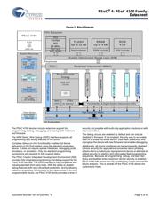
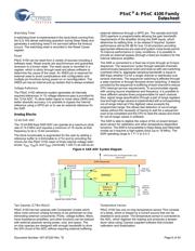
General Description
PSoC
®
4 is a scalable and reconfigurable platform architecture for a family of mixed-signal programmable embedded system
controllers with an ARM
®
Cortex™-M0 CPU. It combines programmable and re-configurable analog and digital blocks with flexible
automatic routing. The PSoC 4100 product family, based on this platform, is a combination of a microcontroller with digital program-
mable logic, high-performance analog-to-digital conversion, opamps with Comparator mode, and standard communication and timing
peripherals. The PSoC 4100 products will be fully upward compatible with members of the PSoC 4 platform for new applications and
design needs. The programmable analog and digital sub-systems allow flexibility and in-field tuning of the design.
Features
32-bit MCU Sub-system
■ 24-MHz ARM Cortex-M0 CPU with single-cycle multiply
■ Up to 32 kB of flash with Read Accelerator
■ Up to 4 kB of SRAM
Programmable Analog
■ Two opamps with reconfigurable high-drive external and
high-bandwidth internal drive and Comparator modes and ADC
input buffering capability
■ 12-bit 806 Ksps SAR ADC with differential and single-ended
modes and Channel Sequencer with signal averaging
■ Two current DACs (IDACs) for general-purpose or capacitive
sensing applications on any pin
■ Two low-power comparators that operate in Deep Sleep
Low Power 1.71-V to 5.5-V operation
■ 20-nA Stop Mode with GPIO pin wakeup
■ Hibernate and Deep Sleep modes allow wakeup-time versus
power trade-offs
Capacitive Sensing
■ Cypress CapSense Sigma-Delta (C"Five different packa-
gesSD) provides best-in-class SNR (>5:1) and water tolerance
■ Cypress supplied software component makes capacitive
sensing design easy
■ Automatic hardware tuning (SmartSense™)
Segment LCD Drive
■ LCD drive supported on all pins (common or segment)
■ Operates in Deep Sleep mode with 4 bits per pin memory
Serial Communication
■ Two independent run-time reconfigurable serial communi-
cation blocks (SCBs) with reconfigurable I
2
C, SPI, or UART
functionality
Timing and Pulse-Width Modulation
■ Four 16-bit timer/counter pulse-width modulator (TCPWM)
blocks
■ Center-aligned, Edge, and Pseudo-random modes
■ Comparator-based triggering of Kill signals for motor drive and
other high reliability digital logic applications
Up to 36 Programmable GPIOs
■ Any GPIO pin can be CapSense, LCD, analog, or digital
■ Drive modes, strengths, and slew rates are programmable
Five different packages
■ 48-pin TQFP, 44-pin TQFP, 40-pin QFN, 35-ball WLCSP, and
28-pin SSOP package
■ 35-ball WLCSP package is shipped with I
2
C Bootloader in
Flash
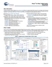
PSoC Creator Design Environment
■ Integrated Development Environment provides schematic
design entry and build (with analog and digital automatic
routing)
■ Applications Programming Interface (API Component) for all
fixed-function and programmable peripherals
Industry Standard Tool Compatibility
■ After schematic entry, development can be done with
ARM-based industry-standard development tools
器件 Datasheet 文档搜索
AiEMA 数据库涵盖高达 72,405,303 个元件的数据手册,每天更新 5,000 多个 PDF 文件
