Datasheet 搜索 > 放大器IC与RF模块 > ADI(亚德诺) > HMC516LC5 数据手册 > HMC516LC5 用户编程技术手册 1/12 页
 器件3D模型
¥ 249.011
HMC516LC5 用户编程技术手册 - ADI(亚德诺)
制造商:
ADI(亚德诺)
分类:
放大器IC与RF模块
封装:
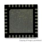
QFN-32
描述:
ANALOG DEVICES HMC516LC5 芯片, 射频放大器, 20.5DB, 18GHZ, 3V, HQFN-32
Pictures:
3D模型
符号图
焊盘图
引脚图
产品图
页面导航:
导航目录
HMC516LC5数据手册
Page:
of 12 Go
若手册格式错乱,请下载阅览PDF原文件
For price, delivery and to place orders: Hittite Microwave Corporation, 2 Elizabeth Drive, Chelmsford, MA 01824
Phone: 978-250-3343 Fax: 978-250-3373 Order On-line at www.hittite.com
Application Support: Phone: 978-250-3343 or apps@hittite.com
MUX & DEMUX - SMT
1
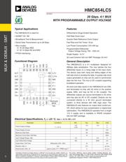
HMC8 54LC5
v04.0614
28 Gbps, 4:1 MUX
WITH PROGRAMMABLE OUTPUT VOLTAGE
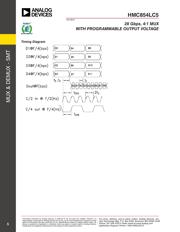
The HMC854LC5 is a 4:1 multiplexer designed for
28Gbps data serialization. The mux latches the four
differential inputs on a rising edge of the input clock.
The device uses both rising and falling edges of the
half-rate clock to serialize the data. A quarter-rate clock
output generated on chip can be used to synchronize
data into the mux. The mux is DC coupled supporting
broadband operation.
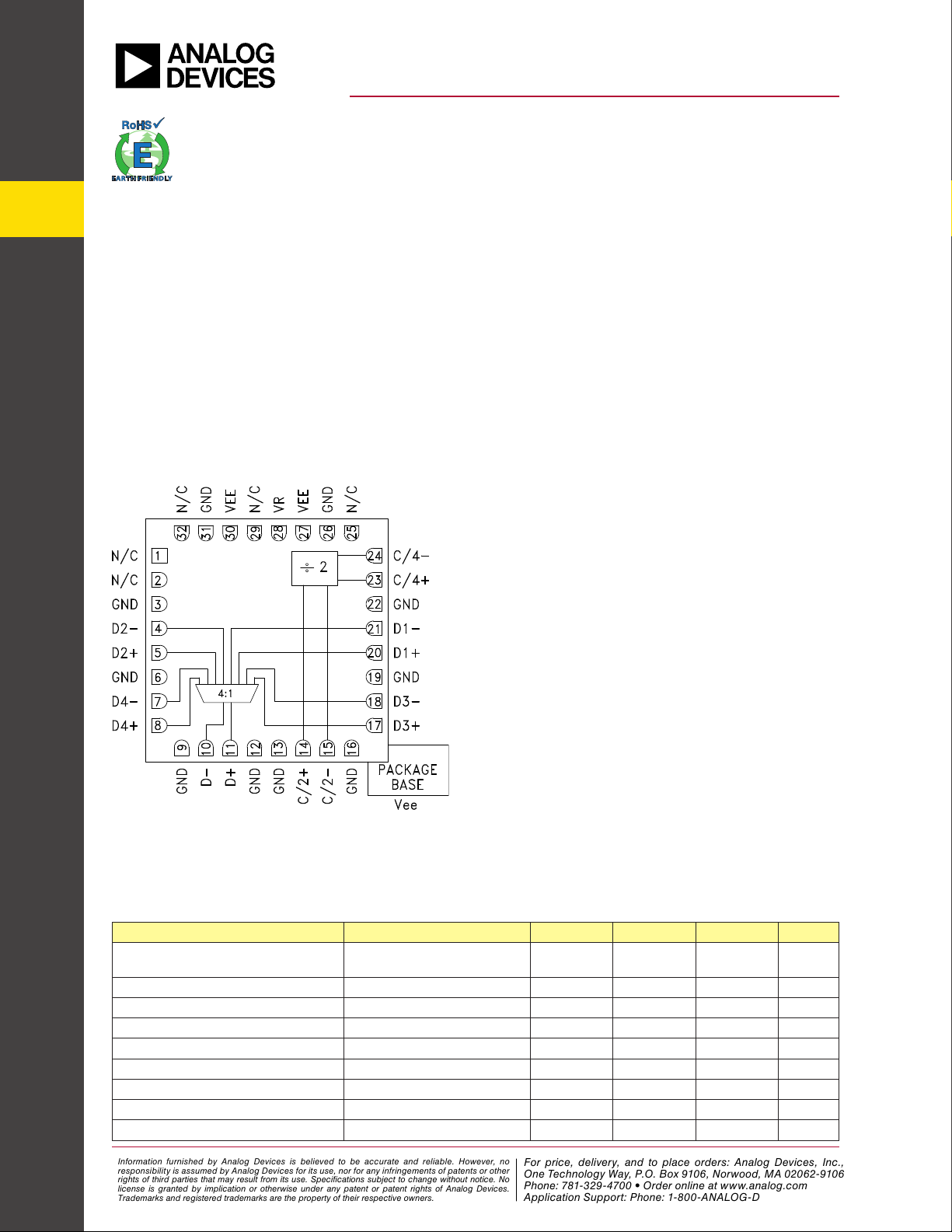
All clock and data inputs to the HMC854LC5 are CML
and terminated on-chip with 50 ohms to the positive
supply, GND, and may be DC or AC coupled. The
differential outputs are source terminated to 50 ohms
and may also be AC or DC coupled. Outputs can be
connected directly to a 50 ohm ground terminated
system, or drive devices with CML logic input. The
HMC854LC5 also features an output level control pin,
VR, which allows for loss compensation or signal level
optimization. The HMC854LC5 operates from a single
-3.3 V supply and is available in ROHS compliant
5x5 mm SMT package.
General Description
Features
Functional Diagram
Differential & Singe-Ended Operation
Half Rate Clock Input
Quarter Rate Reference Clock Output
Fast Rise and Fall Times: 16 ps
Low Power Consumption: 510 mW typ.
Programmable Differential
Output Voltage Swing: 700 - 1250 mV
Single Supply: -3.3 V
32 Lead Ceramic 5x5 mm SMT Package: 25 mm
2
Typical Applications
The HMC854LC5 is ideal for:
• SONET OC 192
• Broadband Test & Measurement
• Serial Data Transmission up to 28 Gbps
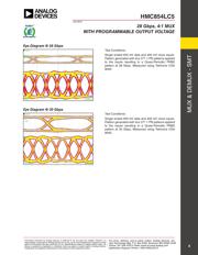
• Mux modes:
4:1 @ 28 Gbps NRZ,
2:1 @ 14 Gbps RZ and NRZ
• FPGA Interfacing
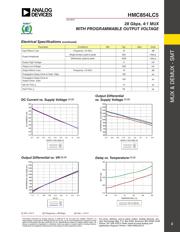
Electrical Specications, T
A
= +25 °C, Vee = -3.3 V, VR = 0 V
Parameter Conditions Min. Typ. Max Units
Power Supply Voltage
T > 75 °C
-3.6
-3.45
-3.3 -3.0 V
V
Power Supply Current 155 mA
Maximum Data Rate 28 Gbps
Maximum Clock Rate, Half Rate 14 GHz
Input Voltage Range, CML -1.5 0.5 V
Input Differential Voltage 100 2000 mV
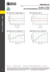
Output Rise / Fall Time Differential, 20% - 80% 16 ps
Random Jitter Jr rms 0.5 ps rms
Deterministic Jitter, Jd peak-to-peak, 2
15
-1 PRBS input
[1]
4 ps, p-p
Information furnished by Analog Devices is believed to be accurate and reliable. However, no
responsibility is assumed by Analog Devices for its use, nor for any infringements of patents or other
rights of third parties that may result from its use. Specifications subject to change without notice. No
license is granted by implication or otherwise under any patent or patent rights of Analog Devices.
Trademarks and registered trademarks are the property of their respective owners.
For price, delivery, and to place orders: Analog Devices, Inc.,
One Technology Way, P.O. Box 9106, Norwood, MA 02062-9106
Phone: 781-329-4700 • Order online at www.analog.com
Application Support: Phone: 1-800-ANALOG-D
器件 Datasheet 文档搜索
AiEMA 数据库涵盖高达 72,405,303 个元件的数据手册,每天更新 5,000 多个 PDF 文件
