Datasheet 搜索 > DC/DC转换器 > ON Semiconductor(安森美) > NCP1252BDR2G 数据手册 > NCP1252BDR2G 用户编程技术手册 1/28 页
 器件3D模型
¥ 3.232
NCP1252BDR2G 用户编程技术手册 - ON Semiconductor(安森美)
制造商:
ON Semiconductor(安森美)
分类:
DC/DC转换器
封装:
SOIC-8
描述:
PWM控制器
Pictures:
3D模型
符号图
焊盘图
引脚图
产品图
页面导航:
引脚图在P1P6Hot
典型应用电路图在P1
原理图在P7
封装尺寸在P28
焊盘布局在P28
型号编码规则在P1P27P28
标记信息在P1
封装信息在P27
技术参数、封装参数在P27
应用领域在P1
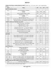
电气规格在P3P4P5
型号编号列表在P2
导航目录
NCP1252BDR2G数据手册
Page:
of 28 Go
若手册格式错乱,请下载阅览PDF原文件
© Semiconductor Components Industries, LLC, 2011
December, 2011 − Rev. 1
1 Publication Order Number:
NCP1611/D
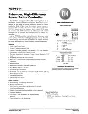
NCP1611
Enhanced, High-Efficiency
Power Factor Controller
The NCP1611 is designed to drive PFC boost stages based on an
innovative Current Controlled Frequency Fold−back (CCFF)
method. In this mode, the circuit classically operates in Critical
conduction Mode (CrM) when the inductor current exceeds a
programmable value. When the current is below this preset level, the
NCP1611 linearly decays the frequency down to about 20 kHz when
the current is null. CCFF maximizes the efficiency at both nominal
and light load. In particular, the stand−by losses are reduced to a
minimum.
Like in FCCrM controllers, internal circuitry allows near−unity
power factor even when the switching frequency is reduced. Housed in
a SO−8 package, the circuit also incorporates the features necessary
for robust and compact PFC stages, with few external components.
Features
• Near−Unity Power Factor
• Critical Conduction Mode (CrM)
• Current Controlled Frequency Fold−back (CCFF): Low Frequency
Operation is Forced at Low Current Levels
• On−time Modulation to Maintain a Proper Current Shaping in CCFF
Mode
• Skip Mode Near the Line Zero Crossing
• Fast Line / Load Transient Compensation (Dynamic Response
Enhancer)
• Valley Turn on
• High Drive Capability: −500 mA / +800 mA
• V
CC
Range: from 9.5 V to 35 V
• Low Start−up Consumption
• A Version: Low V
CC
Start−up Level (10.5 V), B Version: High V
CC
Start−up level (17.0 V)
• Line Range Detection
• This is a Pb−Free Device
Safety Features
• Non−latching, Over−Voltage Protection
• Brown−Out Detection
• Soft−Start for Smooth Start−up Operation (A version)
• Over Current Limitation
• Disable Protection if the Feedback Pin is Not Connected
• Thermal Shutdown
• Low Duty−Cycle Operation if the Bypass Diode is
Shorted
• Open Ground Pin Fault Monitoring
Typical Applications
• PC Power Supplies
• All Off Line Appliances Requiring Power Factor
Correction
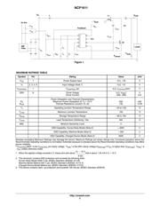
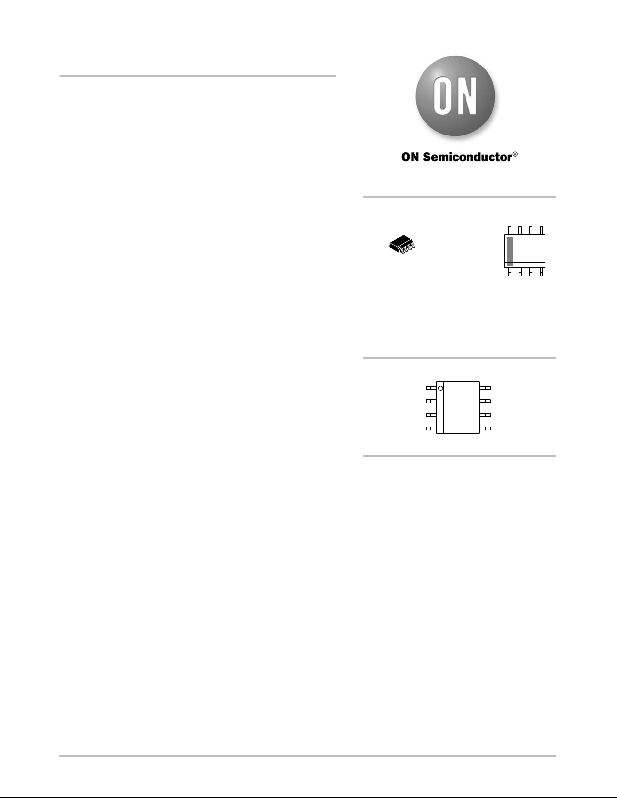
SOIC−8
CASE 751
SUFFIX D
PIN CONNECTIONS
MARKING
DIAGRAM
(Top View)
http://onsemi.com
1
8
NCP1611x = Specific Device Code
x = A or B
A = Assembly Location
L = Wafer Lot
Y = Year
W = Work Week
G = Pb−Free Package
NCP1611x
ALYW
G
1
8
See detailed ordering and shipping information in the package
dimensions section on page 27 of this data sheet.
ORDERING INFORMATION
Feedback
V
CC
DRV
GND
V
control
V
sense
FF
control
CS/ZCD
1
器件 Datasheet 文档搜索
AiEMA 数据库涵盖高达 72,405,303 个元件的数据手册,每天更新 5,000 多个 PDF 文件
