Datasheet 搜索 > 电源监控芯片 > ON Semiconductor(安森美) > NCP302LSN20T1 数据手册 > NCP302LSN20T1 用户编程技术手册 1/27 页

¥ 0
NCP302LSN20T1 用户编程技术手册 - ON Semiconductor(安森美)
制造商:
ON Semiconductor(安森美)
分类:
电源监控芯片
封装:
SOT-23-5
描述:
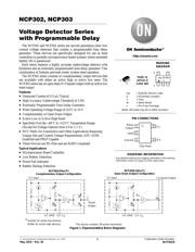
电压检测器系列具有可编程延迟 Voltage Detector Series with Programmable Delay
Pictures:
3D模型
符号图
焊盘图
引脚图
产品图
页面导航:
引脚图在P1Hot
典型应用电路图在P1
原理图在P1
封装尺寸在P26
焊盘布局在P26
型号编码规则在P1P22P23P24P25P27
标记信息在P1P22P23P24P25P26P27
封装信息在P22P23P24P25
技术参数、封装参数在P22P23P24P25
应用领域在P1P22P23P24P25
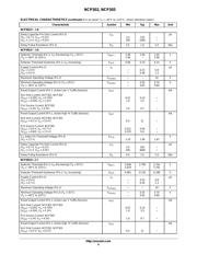
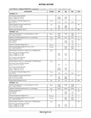
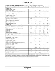
电气规格在P3P4P5P6
型号编号列表在P2
导航目录
NCP302LSN20T1数据手册
Page:
of 27 Go
若手册格式错乱,请下载阅览PDF原文件
© Semiconductor Components Industries, LLC, 2014
May, 2014 − Rev. 26
1 Publication Order Number:
NCP302/D
NCP302, NCP303
Voltage Detector Series
with Programmable Delay
The NCP302 and NCP303 series are second generation ultra−low
current voltage detectors that contain a programmable time delay
generator. These devices are specifically designed for use as reset
controllers in portable microprocessor based systems where extended
battery life is paramount.
Each series features a highly accurate undervoltage detector with
hysteresis and an externally programmable time delay generator. This
combination of features prevents erratic system reset operation.
The NCP302 series consists of complementary output devices that
are available with either an active high or active low reset. The
NCP303 series has an open drain N−Channel output with an active low
reset output.
Features
• Quiescent Current of 0.5 mA Typical
• High Accuracy Undervoltage Threshold of 2.0%
• Externally Programmable Time Delay Generator
• Wide Operating Voltage Range of 0.8 V to 10 V
• Complementary or Open Drain Output
• Active Low or Active High Reset
• Specified Over the −40°C to +125°C Temperature Range
(Except for Voltage Options from 0.9 to 1.1 V)
• NCV Prefix for Automotive and Other Applications Requiring
Unique Site and Control Change Requirements; AEC−Q100
Qualified and PPAP Capable
• These Devices are Pb−Free and are RoHS Compliant
Typical Applications
• Microprocessor Reset Controller
• Low Battery Detection
• Power Fail Indicator
• Battery Backup Detection
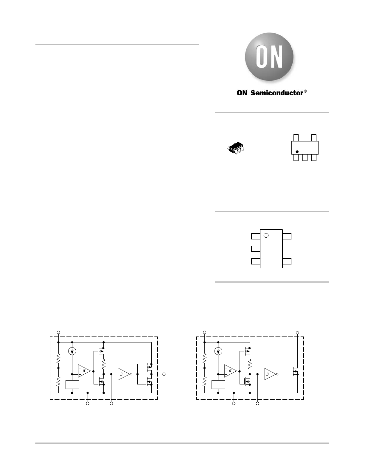
Figure 1. Representative Block Diagrams
This device contains 28 active transistors.
NCP303LSNxxT1
Open Drain Output Configuration
NCP302xSNxxT1
Complementary Output Configuration
* Inverter for active low devices.
* Buffer for active high devices.
V
ref
2 Input
1
Reset
Output
3 GND
5C
D
R
D
*
V
ref
2 Input
3 GND
5C
D
R
D
1 Reset Outp
ut
See detailed ordering and shipping information in the ordering
information section on page 22 of this data sheet.
ORDERING INFORMATION
TSOP−5/
SOT23−5
CASE 483
PIN CONNECTIONS
1
3
N.C.
Reset
Output
2
Input
Ground
4
C
D
5
(Top View)
http://onsemi.com
1
5
xxx AYWG
G
MARKING
DIAGRAM
xxx = Specific Device Code
A = Assembly Location
Y = Year
W = Work Week
G = Pb−Free Package
1
5
(Note: Microdot may be in either location)
器件 Datasheet 文档搜索
AiEMA 数据库涵盖高达 72,405,303 个元件的数据手册,每天更新 5,000 多个 PDF 文件
