Datasheet 搜索 > ON Semiconductor(安森美) > NCV1117DT33T4G 数据手册 > NCV1117DT33T4G 用户编程技术手册 1/17 页


¥ 1.181
NCV1117DT33T4G 用户编程技术手册 - ON Semiconductor(安森美)
制造商:
ON Semiconductor(安森美)
封装:
TO-252-3
描述:
低压差稳压器 ANA 1.0 LDO REGULATOR
Pictures:
3D模型
符号图
焊盘图
引脚图
产品图
页面导航:
引脚图在P1Hot
典型应用电路图在P2
封装尺寸在P16P17
焊盘布局在P16P17
型号编码规则在P1P12P13P17
标记信息在P1P14P15P17
封装信息在P12P13
技术参数、封装参数在P12P13
应用领域在P1P2P9P12P13
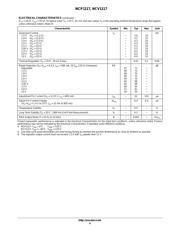
电气规格在P3P4
型号编号列表在P2
导航目录
NCV1117DT33T4G数据手册
Page:
of 17 Go
若手册格式错乱,请下载阅览PDF原文件
© Semiconductor Components Industries, LLC, 2014
September, 2014 − Rev. 27
1 Publication Order Number:
NCP1117/D
NCP1117, NCV1117
1.0 A Low-Dropout Positive
Fixed and Adjustable
Voltage Regulators
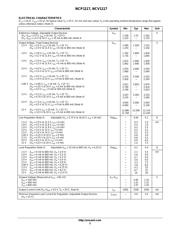
The NCP1117 series are low dropout positive voltage regulators that
are capable of providing an output current that is in excess of 1.0 A
with a maximum dropout voltage of 1.2 V at 800 mA over
temperature. This series contains nine fixed output voltages of 1.5 V,
1.8 V, 1.9 V, 2.0 V, 2.5 V, 2.85 V, 3.3 V, 5.0 V, and 12 V that have no
minimum load requirement to maintain regulation. Also included is an
adjustable output version that can be programmed from 1.25 V to
18.8 V with two external resistors. On chip trimming adjusts the
reference/output voltage to within ±1.0% accuracy. Internal protection
features consist of output current limiting, safe operating area
compensation, and thermal shutdown. The NCP1117 series can
operate with up to 20 V input. Devices are available in SOT−223 and
DPAK packages.
Features
• Output Current in Excess of 1.0 A
• 1.2 V Maximum Dropout Voltage at 800 mA Over Temperature
• Fixed Output Voltages of 1.5 V, 1.8 V, 1.9 V, 2.0 V, 2.5 V, 2.85 V,
3.3 V, 5.0 V, and 12 V
• Adjustable Output Voltage Option
• No Minimum Load Requirement for Fixed Voltage Output Devices
• Reference/Output Voltage Trimmed to ±1.0%
• Current Limit, Safe Operating and Thermal Shutdown Protection
• Operation to 20 V Input
• NCV Prefix for Automotive and Other Applications Requiring
Unique Site and Control Change Requirements; AEC−Q100
Qualified and PPAP Capable
• These are Pb-Free Devices
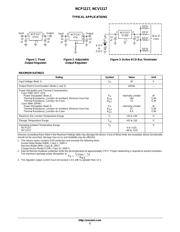
Applications
• Consumer and Industrial Equipment Point of Regulation
• Active SCSI Termination for 2.85 V Version
• Switching Power Supply Post Regulation
• Hard Drive Controllers
• Battery Chargers
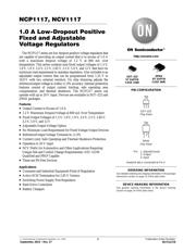
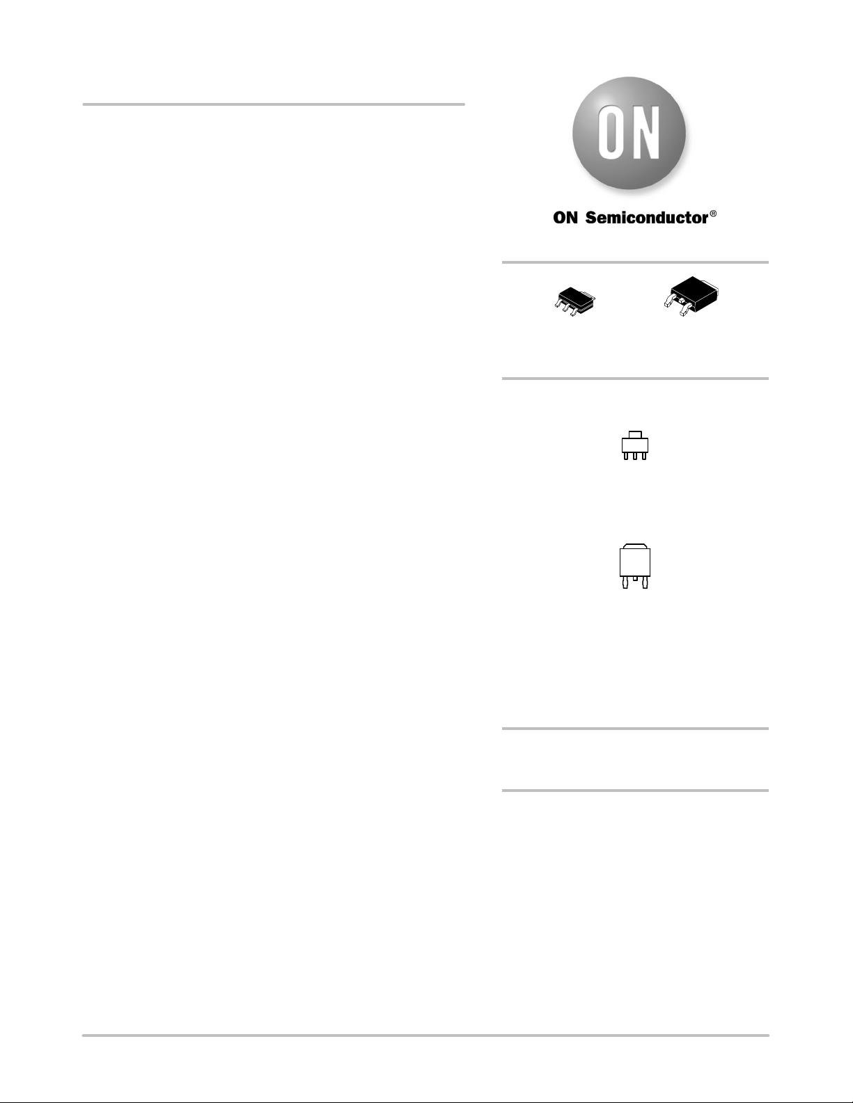
SOT−223
ST SUFFIX
CASE 318H
DPAK
DT SUFFIX
CASE 369C
Pin: 1. Adjust/Ground
2. Output
3. Input
Heatsink tab is connected to Pin 2.
See detailed ordering and shipping information in the package
dimensions section on page 12 of this data sheet.
ORDERING INFORMATION
See general marking information in the device marking
section on page 14 of this data sheet.
DEVICE MARKING INFORMATION
1 23
1
2
3
Tab
Tab
http://onsemi.com
PIN CONFIGURATION
SOT−223
(Top View)
DPAK
(Top View)
器件 Datasheet 文档搜索
AiEMA 数据库涵盖高达 72,405,303 个元件的数据手册,每天更新 5,000 多个 PDF 文件
