Datasheet 搜索 > 微控制器 > Microchip(微芯) > PIC18F46K40-I/MV 数据手册 > PIC18F46K40-I/MV 用户编程技术手册 1/44 页
 器件3D模型
¥ 1.99
PIC18F46K40-I/MV 用户编程技术手册 - Microchip(微芯)
制造商:
Microchip(微芯)
分类:
微控制器
封装:
UQFN-40
描述:
PIC 64MHz 闪存:32K@x16bit
Pictures:
3D模型
符号图
焊盘图
引脚图
产品图
页面导航:
导航目录
PIC18F46K40-I/MV数据手册
Page:
of 44 Go
若手册格式错乱,请下载阅览PDF原文件
2014-2015 Microchip Technology Inc. DS40001772B-page 1
PIC18(L)F2X/4XK40
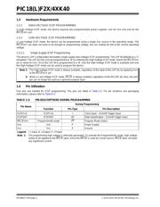
1.0 OVERVIEW
This programming specification describes an SPI-based programming method for the PIC18(L)F2X/4XK40 family of
microcontrollers. Section 3.0 “Programming Algorithms” describes the programming commands, programming
algorithms and electrical specifications which are used in that particular programming method. Appendix B contains
individual part numbers, device identification and checksum values, pinout and packaging information, and
Configuration Words.
1.1 Programming Data Flow
Nonvolatile Memory (NVM) programming data can be supplied by either the high-voltage In-Circuit Serial
Programming™ (ICSP™) interface or the low-voltage In-Circuit Serial Programming (ICSP) interface. Data can be
programmed into the Program Flash Memory (PFM), Data EEPROM Memory, dedicated “User ID” locations and the
Configuration Words.
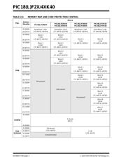
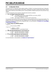
1.2 Write and/or Erase Selection
Erasing or writing is selected according to the command used to begin operation (see Table 3-1). The terminologies used
in this document, related to erasing/writing to the program memory, are defined in Table 1-1 and are detailed below.
1.2.1 ERASING MEMORY
Memory is erased by row or in bulk, where ‘bulk’ includes many subsets of the total memory space. The duration of the
erase is determined by the size of program memory. All Bulk ICSP Erase commands have minimum V
DD
requirements,
which are higher than the Row Erase and write requirements.
1.2.2 WRITING MEMORY
Memory is written one row at a time. Multiple load data for NVM commands is used to fill the row data latches. The
duration of the write can be determined either internally or externally.
1.2.3 MULTI-WORD PROGRAMMING INTERFACE
Program Flash Memory (PFM) panels include up to a 64-word (one row) programming interface. Refer to Table 3-3 for
row size of erase and write operations for the PIC18(L)F2X/4XK40 family. The row to be programmed must first be
erased, either with a Bulk Erase or a Row Erase.
Note 1: This is a SPI-compatible programming method with 8-bit commands.
2: The low-voltage entry code is now 32 clocks and MSb first, unlike previous PIC18 devices which had
33 clocks and LSb first.
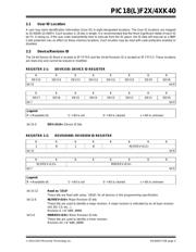
TABLE 1-1: PROGRAMMING TERMS
Term Definition
Programmed Cell A memory cell at logic ‘0’
Erased Cell A memory cell at logic ‘1’
Erase Change memory cell from a ‘0’ to a ‘1’
Write Change memory cell from a ‘1’ to a ‘0’
Program Generic erase and/or write
PIC18(L)F2X/4XK40 Memory Programming Specification
器件 Datasheet 文档搜索
AiEMA 数据库涵盖高达 72,405,303 个元件的数据手册,每天更新 5,000 多个 PDF 文件
