Datasheet 搜索 > EEPROM芯片 > Xilinx(赛灵思) > XC18V02PCG44C0100 数据手册 > XC18V02PCG44C0100 用户编程技术手册 3/25 页

 器件3D模型
¥ 80.664
XC18V02PCG44C0100 用户编程技术手册 - Xilinx(赛灵思)
制造商:
Xilinx(赛灵思)
分类:
EEPROM芯片
封装:
LCC-44
Pictures:
3D模型
符号图
焊盘图
引脚图
产品图
页面导航:
导航目录
XC18V02PCG44C0100数据手册
Page:
of 25 Go
若手册格式错乱,请下载阅览PDF原文件

XC18V00 Series In-System-Programmable Configuration PROMs
DS026 (v6.0) August 5, 2015 www.xilinx.com
Product Specification 3
R
— PRODUCT OBSOLETE / UNDER OBSOLESCENCE —
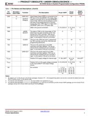
CEO 12 DATA OUT Chip Enable Output (CEO) is connected to the
CE
input of the next PROM in the chain. This
output is Low when CE
is Low and OE/RESET
input is High, AND the internal address counter
has been incremented beyond its Terminal
Count (TC) value. CEO
returns to High when
OE/RESET
goes Low or CE goes High.
21 27 13
11 OUTPUT
ENABLE
GND GND is the ground connection. 6, 18, 28 & 41 3, 12, 24 &
34
11
TMS MODE
SELECT
The state of TMS on the rising edge of TCK
determines the state transitions at the Test
Access Port (TAP) controller. TMS has an
internal 50 kΩ resistive pull-up to provide a
logic 1 to the device if the pin is not driven.
5115
TCK CLOCK This pin is the JTAG test clock. It sequences
the TAP controller and all the JTAG test and
programming electronics.
7136
TDI DATA IN This pin is the serial input to all JTAG
instruction and data registers. TDI has an
internal 50 kΩ resistive pull-up to provide a
logic 1 to the device if the pin is not driven.
394
TDO DATA OUT This pin is the serial output for all JTAG
instruction and data registers. TDO has an
internal 50 kΩ resistive pull-up to provide a
logic 1 to the system if the pin is not driven.
31 37 17
V
CCINT
Positive 3.3V supply voltage for internal logic. 17, 35 & 38
(3)
23, 41 &
44
(3)
18 & 20
(3)
V
CCO
Positive 3.3V or 2.5V supply voltage connected
to the input buffers
(2)
and output voltage
drivers.
8, 16, 26 & 36 14, 22, 32 &
42
19
NC No connects. 1, 2, 4,
11, 12, 20, 22,
23, 24, 30, 32,
33, 34, 37, 39,
44
1, 6, 7, 8,
10, 17, 18,
26, 28, 29,
30, 36, 38,
39, 40, 43
Notes:
1. By default, pin 7 is the D4 pin in the 20-pin packages. However, CF → D4 programming option can be set to override the default and route
the CF function to pin 7 in the Serial mode.
2. For devices with IDCODES 0502x093h, the input buffers are supplied by V
CCINT
.
3. For devices with IDCODES 0503x093h, the following V
CCINT
pins are no-connects: pin 38 in 44-pin VQFP package, pin 44 in 44-pin PLCC
package, and pin 20 in 20-pin SOIC and 20-pin PLCC packages.
Table 1: Pin Names and Descriptions (Cont’d)
Pin
Name
Boundary-
Scan Order
Function Pin Description 44-pin VQFP
44-pin
PLCC
20-pin
SOIC &
PLCC
器件 Datasheet 文档搜索
AiEMA 数据库涵盖高达 72,405,303 个元件的数据手册,每天更新 5,000 多个 PDF 文件


