Datasheet 搜索 > 存储芯片 > Xilinx(赛灵思) > XCF32P-FSG48C 数据手册 > XCF32P-FSG48C 用户编程技术手册 4/35 页

¥ 0
XCF32P-FSG48C 用户编程技术手册 - Xilinx(赛灵思)
制造商:
Xilinx(赛灵思)
分类:
存储芯片
Pictures:
3D模型
符号图
焊盘图
引脚图
产品图
页面导航:
引脚图在P24P25P26P27P28Hot
原理图在P2P34
型号编码规则在P30
标记信息在P30P31P34
封装信息在P13
技术参数、封装参数在P13P24P33P35
应用领域在P35
电气规格在P1P13P16P33
导航目录
XCF32P-FSG48C数据手册
Page:
of 35 Go
若手册格式错乱,请下载阅览PDF原文件

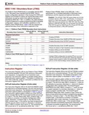
Platform Flash In-System Programmable Configuration PROMs
DS123 (v2.18) May 19, 2010 www.xilinx.com
Product Specification 4
R
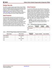
Design Security
The Xilinx in-system programmable Platform Flash PROM
devices incorporate advanced data security features to fully
protect the FPGA programming data against unauthorized
reading via JTAG. The XCFxxP PROMs can also be
programmed to prevent inadvertent writing via JTAG.
Tabl e 3 and Ta bl e 4 show the security settings available for
the XCFxxS PROM and XCFxxP PROM, respectively.
Read Protection
The read protect security bit can be set by the user to
prevent the internal programming pattern from being read or
copied via JTAG. Read protection does not prevent write
operations. For the XCFxxS PROM, the read protect
security bit is set for the entire device, and resetting the read
protect security bit requires erasing the entire device. For
the XCFxxP PROM the read protect security bit can be set
for individual design revisions, and resetting the read
protect bit requires erasing the particular design revision.
Write Protection
The XCFxxP PROM device also allows the user to write
protect (or lock) a particular design revision or PROM option
settings. Write protection helps to prevent an inadvertent
JTAG instruction from modifying an area by write protecting
the area and by locking the erase instruction. The write-
protection setting can be cleared by erasing the protected
area. However, an XSC_UNLOCK instruction must first be
issued to the XCFxxP PROM to unlock the ISC_ERASE
instruction. Refer to the XCFxxP PROM BSDL file for the
XSC_UNLOCK and ISC_ERASE instructions.
Caution!
The iMPACT software always issues a
XSC_UNLOCK when performing an Erase operation on an
XCFxxP PROM and, thus, always unlocks the write
protection.
Tabl e 3 : XCFxxS Device Data Security Options
Read Protect
Read/Verify
Inhibited
Program
Inhibited
Erase
Inhibited
Reset (default)
Set
3
Tabl e 4: XCFxxP Design Revision Data Security Options
Read Protect Write Protect
Read/Verify
Inhibited
Program Inhibited Erase Inhibited
Reset (default) Reset (default)
Reset (default) Set
33
Set Reset (default)
3
Set Set
333
器件 Datasheet 文档搜索
AiEMA 数据库涵盖高达 72,405,303 个元件的数据手册,每天更新 5,000 多个 PDF 文件

