Datasheet 搜索 > EEPROM芯片 > Xilinx(赛灵思) > XCF32PVOG48C 数据手册 > XCF32PVOG48C 用户编程技术手册 1/36 页
 器件3D模型
¥ 242.723
XCF32PVOG48C 用户编程技术手册 - Xilinx(赛灵思)
制造商:
Xilinx(赛灵思)
分类:
EEPROM芯片
封装:
TSOP-48
描述:
XCFxx 配置闪存XCFxx 系列闪存 EPROM 提供易于使用、经济有效和可重新编程方法,用于存储大 Xilinx FPGA 配置比特流。 系统内可编程闪存设备用于配置 Xilinx FPGA IEEE 标准 1149.1/1532 边界扫描 (JTAG) 支持,用于编程、原型设计和测试 级联,用于存储较长或多个比特流 输入/输出引脚,与 +1.5V 至 +3.3V 的电压级别范围兼容 ### Configuration Memory, Xilinx
Pictures:
3D模型
符号图
焊盘图
引脚图
产品图
页面导航:
引脚图在P24P25P26P27P28Hot
原理图在P2P34
型号编码规则在P30
标记信息在P30P31P34
封装信息在P13
技术参数、封装参数在P13P24P33
电气规格在P1P13P16P33

导航目录
XCF32PVOG48C数据手册
Page:
of 36 Go
若手册格式错乱,请下载阅览PDF原文件
DS123 (v2.19) June 6, 2016 www.xilinx.com
Product Specification 1
© Copyright 2003–2016 Xilinx, Inc. XILINX, the Xilinx logo, Artix, ISE, Kintex, Spartan, Virtex, Vivado, Zynq, and other designated brands included herein are trademarks of Xilinx
in the United States and other countries. All other trademarks are the property of their respective owners.
Features
• In-System Programmable PROMs for Configuration of
Xilinx® FPGAs
• Low-Power Advanced CMOS NOR Flash Process
• Endurance of 20,000 Program/Erase Cycles
• Operation over Full Industrial Temperature Range
(–40°C to +85°C)
• IEEE Standard 1149.1/1532 Boundary-Scan (JTAG)
Support for Programming, Prototyping, and Testing
• JTAG Command Initiation of Standard FPGA
Configuration
• Cascadable for Storing Longer or Multiple Bitstreams
• Dedicated Boundary-Scan (JTAG) I/O Power Supply (V
CCJ
)
• I/O Pins Compatible with Voltage Levels Ranging From
1.8V to 3.3V
• Design Support Using the Xilinx ISE® Alliance and
Foundation™ Software Packages
• XCF01S/XCF02S/XCF04S
• 3.3V Supply Voltage
• Serial FPGA Configuration Interface
• Available in Small-Footprint VO20 and VOG20
Packages
• XCF08P/XCF16P/XCF32P
• 1.8V Supply Voltage
• Serial or Parallel FPGA Configuration Interface
• Available in Small-Footprint VOG48, FS48, and
FSG48 Packages
• Design Revision Technology Enables Storing and
Accessing Multiple Design Revisions for
Configuration
• Built-In Data Decompressor Compatible with Xilinx
Advanced Compression Technology
Description
Xilinx introduces the Platform Flash series of in-system
programmable configuration PROMs. Available in
1 to 32 Mb densities, these PROMs provide an easy-to-use,
cost-effective, and reprogrammable method for storing large
Xilinx FPGA configuration bitstreams. The Platform Flash
PROM series includes both the 3.3V XCFxxS PROM and
the 1.8V XCFxxP PROM. The XCFxxS version includes
4 Mb, 2 Mb, and 1 Mb PROMs that support Master Serial
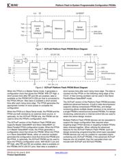
and Slave Serial FPGA configuration modes (Figure 1,
page 2). The XCFxxP version includes 32 Mb, 16 Mb, and
8 Mb PROMs that support Master Serial, Slave Serial,
Master SelectMAP, and Slave SelectMAP FPGA
configuration modes (Figure 2, page 2).
When driven from a stable, external clock, the PROMs can
output data at rates up to 33 MHz. Refer to "AC Electrical
Characteristics," page 16 for timing considerations.
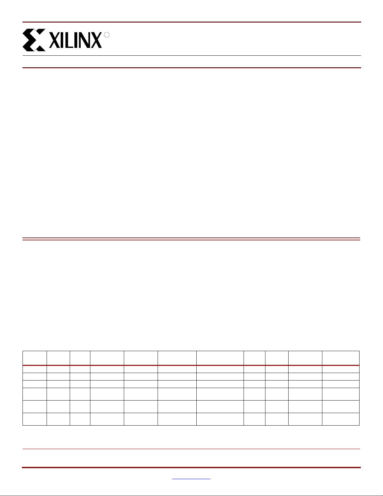
A summary of the Platform Flash PROM family members
and supported features is shown in Table 1.
35
Platform Flash In-System Programmable
Configuration PROMs
DS123 (v2.19) June 6, 2016 Product Specification
R
Table 1: Platform Flash PROM Features
Device
Density
(Mb)
V
CCINT
(V)
V
CCO
Range
(V)
V
CCJ
Range
(V)
Packages
Program In-system
via JTAG
Serial
Config.
Parallel
Config.
Design
Revisioning
Compression
XCF01S 1 3.3 1.8 – 3.3 2.5 – 3.3 VO20/VOG20
XCF02S 2 3.3 1.8 – 3.3 2.5 – 3.3 VO20/VOG20
XCF04S 4 3.3 1.8 – 3.3 2.5 – 3.3 VO20/VOG20
XCF08P 8 1.8 1.8 – 3.3 2.5 – 3.3
VO48/VOG48
FS48/FSG48
(1)
XCF16P 16 1.8 1.8 – 3.3 2.5 – 3.3
VO48/VOG48
FS48/FSG48
XCF32P 32 1.8 1.8 – 3.3 2.5 – 3.3
VO48/VOG48
FS48/FSG48
Notes:
1. XCF08P supports storage of a design revision only when cascaded with another XCFxxP PROM. See "Design Revisioning," page 8 for details.
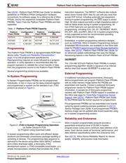
器件 Datasheet 文档搜索
AiEMA 数据库涵盖高达 72,405,303 个元件的数据手册,每天更新 5,000 多个 PDF 文件
