Datasheet 搜索 > EEPROM芯片 > Microchip(微芯) > 24LC024/P 数据手册 > 24LC024/P 开发手册 2/14 页
 器件3D模型
¥ 3.219
24LC024/P 开发手册 - Microchip(微芯)
制造商:
Microchip(微芯)
分类:
EEPROM芯片
封装:
PDIP-8
描述:
24AA32A 系列 32 Kb I2C (4 K X 8) 1.7 V 串行 EEPROM SMT - SOIC-8
Pictures:
3D模型
符号图
焊盘图
引脚图
产品图
页面导航:
功能描述在P2
导航目录
24LC024/P数据手册
Page:
of 14 Go
若手册格式错乱,请下载阅览PDF原文件

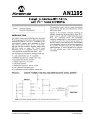
AN1195
DS01195B-page 2 © 2008 Microchip Technology Inc.
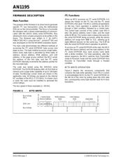
FIRMWARE DESCRIPTION
Main Function
The purpose of the firmware is to show how to generate
specific I
2
C bus transactions using the bidirectional
SDA pin on the microcontroller. The focus is to provide
the designer with a strong understanding of communi-
cation with the 24XXX series serial EEPROMs, thus
allowing for more complex programs to be written in the
future. The firmware was written in C for NXP’s
P89LPC952 MCU using the Keil™ µVision3
®
IDE and
was developed on the Keil MCB950 evaluation board.
The main code demonstrates two different methods of
accessing the I
2
C serial EEPROM: byte access and
page access. The byte method accesses single bytes,
where every data byte is preceded by three bytes of
address: device address, MSB address, and LSB
address. In the page access method, the MCU sends
the address of the first byte, and the I
2
C serial
EEPROM internally increments the address pointer for
the next data byte.
The code was tested using the 24XX512 serial
EEPROM. The EEPROM features 64K x 8 (512 Kbit) of
memory and a page write capability of up to 128 bytes
of data. Oscilloscope screen shots are shown in this
application note. All timings are based on the internal
RC oscillator of the MCU (7.373 MHz). If a faster clock
is used, the code must be modified to generate the
correct delays.
The bus speed in these examples is ~50 kHz.
I
2
C Functions
When an MCU accesses an I
2
C serial EEPROM, it is
always the master on the I
2
C bus and the I
2
C serial
EEPROM is the slave. The MCU controls all operations
on the bus. Each operation is started by the MCU
through a Start condition, followed by a control byte.
The control byte consists of the control code (first 4
bits), the device address (next 3 bits), and the read/
write (R/
W) bit. The control code is always the same for
the serial EEPROM being accessed, while the device
address can range from ‘000’ to ‘111’, allowing up to
eight different devices on the same bus. The R/
W bit
tells the serial EEPROM which operation to perform.
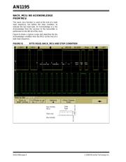
To access an I
2
C serial
EEPROM at the start, the MCU
writes the device address and the byte address to the
I
2
C serial EEPROM; thus, each access cycle starts
with a Write condition. For read operations, after the
above sequence, the MCU switches from Transmitter
mode to Receiver mode and the serial EEPROM from
Receiver to Transmitter mode through a Restart
condition.
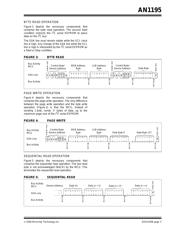
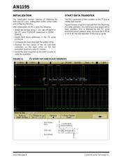
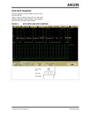
BYTE WRITE OPERATION
Figure 2 depicts the necessary components that
comprise the byte write operation. Each MCU’s action
is acknowledged (ACK) by the I
2
C serial EEPROM on
the 9th bit of the clock by pulling down the SDA data
line; consequently, every byte transfer lasts for 9 clock
transitions.
FIGURE 2: BYTE WRITE
Bus Activity
MCU
SDA Line
Bus Activity
S
T
A
R
T
MSB Address
Byte
LSB Address
Byte
Data Byte
S
T
O
P
A
C
K
A
C
K
A
C
K
A
C
K
S 1010 0
A
2
A
1
A
0
P
Control Byte/
Device Address
器件 Datasheet 文档搜索
AiEMA 数据库涵盖高达 72,405,303 个元件的数据手册,每天更新 5,000 多个 PDF 文件
