Datasheet 搜索 > ADI(亚德诺) > AD6645-80-PCB 数据手册 > AD6645-80-PCB 开发手册 2/20 页


¥ 1839.886
AD6645-80-PCB 开发手册 - ADI(亚德诺)
制造商:
ADI(亚德诺)
Pictures:
3D模型
符号图
焊盘图
引脚图
产品图
AD6645-80-PCB数据手册
Page:
of 20 Go
若手册格式错乱,请下载阅览PDF原文件
REV. B
–2–
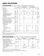
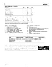
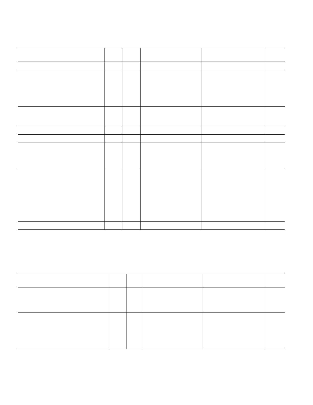
AD6645–SPECIFICATIONS
DC SPECIFICATIONS
Test AD6645ASQ-80 AD6645ASQ-105
Parameter Temp Level Min Typ Max Min Typ Max Unit
RESOLUTION 14 Bits
ACCURACY
No Missing Codes Full II Guaranteed Guaranteed
Offset Error Full II –10 +1.2 +10 –10 +1.2 +10 mV
Gain Error Full II –10 0 +10 –10 0 +10 % FS
Differential Nonlinearity (DNL) Full II –1.0 ±0.25 +1.5 –1.0 ±0.5 +1.5 LSB
Integral Nonlinearity (INL) Full V ±0.5 ±1.5 LSB
TEMPERATURE DRIFT
Offset Error Full V 1.5 1.5 ppm/°C
Gain Error Full V 48 48 ppm/°C
POWER SUPPLY REJECTION (PSRR) 25°CV ±1.0 ±1.0 mV/V
REFERENCE OUT (VREF)
1
Full V 2.4 2.4 V
ANALOG INPUTS (AIN, AIN)
Differential Input Voltage Range Full V 2.2 2.2 V p-p
Differential Input Resistance Full V 1 1 kΩ
Differential Input Capacitance 25°CV 1.5 1.5 pF
POWER SUPPLY
Supply Voltages
AV
CC
Full II 4.75 5.0 5.25 4.75 5.0 5.25 V
DV
CC
Full II 3.0 3.3 3.6 3.0 3.3 3.6 V
Supply Current
I AV
CC
(AV
CC
= 5.0 V) Full II 275 320 275 320 mA
I DV
CC
(DV
CC
= 3.3 V) Full II 32 45 32 45 mA
Rise Time
2
AV
CC
Full IV 250 250 ms
POWER CONSUMPTION Full II 1.5 1.75 1.5 1.75 W
NOTES
1
VREF is provided for setting the common-mode offset of a differential amplifier such as the AD8138 when a dc-coupled analog input is required. VREF should be
buffered if used to drive additional circuit functions.
2
Specified for dc supplies with linear rise time characteristics.
Specifications subject to change without notice
DIGITAL SPECIFICATIONS
Test AD6645ASQ-80 AD6645ASQ-105
Parameter (Conditions) Temp Level Min Typ Max Min Typ Max Unit
ENCODE INPUTS (ENC, ENC)
Differential Input Voltage
1
Full IV 0.4 0.4 V p-p
Differential Input Resistance 25°CV 10 10 kΩ
Differential Input Capacitance 25°CV 2.5 2.5 pF
LOGIC OUTPUTS (D13–D0, DRY, OVR
2
)
Logic Compatibility CMOS CMOS
Logic 1 Voltage (DV
CC
= 3.3 V)
3
Full II 2.85 DV
CC
–2 2.85 DV
CC
–2 V
Logic 0 Voltage (DV
CC
= 3.3 V)
3
Full II 0.2 0.5 0.2 0.5 V
Output Coding Twos Complement Twos Complement
DMID Full V DV
CC
/2 DV
CC
/2 V
NOTES
1
All ac specifications tested by driving ENCODE and ENCODE differentially.
2
The functionality of the Overrange bit is specified for a temperature range of 25°C to 85°C only.
3
Digital output logic levels: DV
CC
= 3.3 V, C
LOAD
= 10 pF. Capacitive loads >10 pF will degrade performance.
Specifications subject to change without notice.
(AV
CC
= 5 V, DV
CC
= 3.3 V; T
MIN
and T
MAX
at rated speed grade, unless otherwise noted.)
(AV
CC
= 5 V, DV
CC
= 3.3 V; T
MIN
and T
MAX
at rated speed grade, unless otherwise noted.)
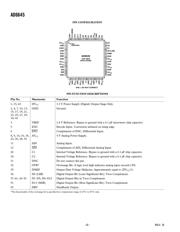
器件 Datasheet 文档搜索
AiEMA 数据库涵盖高达 72,405,303 个元件的数据手册,每天更新 5,000 多个 PDF 文件
