Datasheet 搜索 > ADI(亚德诺) > AD6645-80-PCB 数据手册 > AD6645-80-PCB 开发手册 6/20 页


¥ 1839.886
AD6645-80-PCB 开发手册 - ADI(亚德诺)
制造商:
ADI(亚德诺)
Pictures:
3D模型
符号图
焊盘图
引脚图
产品图
AD6645-80-PCB数据手册
Page:
of 20 Go
若手册格式错乱,请下载阅览PDF原文件
REV. B
–6–
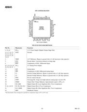
AD6645
PIN CONFIGURATION
52 51 50 49 48 43 42 41 4047 46 45 44
14 15 16 17 18 19 20 21 22 23 24 25 26
1
2
3
4
5
6
7
8
9
10
11
13
12
PIN 1
IDENTIFIER
TOP VIEW
(Not to Scale)
39
38
37
36
35
34
33
32
31
30
29
28
27
AD6645
AV
CC
GND
AV
CC
GND
AV
CC
GND
GND
AV
CC
GND
C2
GND
AV
CC
DRY
D13 (MSB)
D12
D11
D10
D9
D8
D7
DV
CC
GND
D5
D4
DV
CC
GND
VREF
GND
ENC
ENC
GND
AV
CC
AV
CC
GND
AIN
AIN
GND
D3
D2
D1
D0 (LSB)
DMID
GND
DV
CC
OVR
DNC
AV
CC
GND
AV
CC
GND
C1
D6
DNC = DO NOT CONNECT
PIN FUNCTION DESCRIPTIONS
Pin No. Mnemonic Function
1, 33, 43 DV
CC
3.3 V Power Supply (Digital) Output Stage Only.
2, 4, 7, 10, 13, GND Ground.
15, 17, 19, 21,
23, 25, 27, 29,
34, 42
3 VREF 2.4 V Reference. Bypass to ground with a 0.1 µF microwave chip capacitor.
5 ENC Encode Input. Conversion initiated on rising edge.
6 ENC Complement of ENC, Differential Input.
8, 9, 14, 16, 18, AV
CC
5 V Analog Power Supply.
22, 26, 28, 30
11 AIN Analog Input.
12 AIN Complement of AIN, Differential Analog Input.
20 C1 Internal Voltage Reference. Bypass to ground with a 0.1 µF chip capacitor.
24 C2 Internal Voltage Reference. Bypass to ground with a 0.1 µF chip capacitor.
31 DNC Do not connect this pin.
32 OVR* Overrange Bit. A logic level high indicates analog input exceeds ±FS.
35 DMID Output Data Voltage Midpoint. Approximately equal to (DV
CC
)/2.
36 D0 (LSB) Digital Output Bit (Least Significant Bit); Twos Complement.
37–41, 44–50 D1–D5, D6– D12 Digital Output Bits in Twos Complement.
51 D13 (MSB) Digital Output Bit (Most Significant Bit); Twos Complement.
52 DRY DataReady Output.
*The functionality of the overrange bit is specified for a temperature range of 25°C to 85°C only.
器件 Datasheet 文档搜索
AiEMA 数据库涵盖高达 72,405,303 个元件的数据手册,每天更新 5,000 多个 PDF 文件
