Datasheet 搜索 > 放大器、缓冲器 > ADI(亚德诺) > AD8210YRZ 数据手册 > AD8210YRZ 开发手册 1/8 页
 器件3D模型
¥ 28.196
AD8210YRZ 开发手册 - ADI(亚德诺)
制造商:
ADI(亚德诺)
分类:
放大器、缓冲器
封装:
SOIC-8
描述:
Analog Devices
Pictures:
3D模型
符号图
焊盘图
引脚图
产品图
AD8210YRZ数据手册
Page:
of 8 Go
若手册格式错乱,请下载阅览PDF原文件

AN-669
APPLICATION NOTE
One Technology Way • P.O. Box 9106 • Norwood, MA 02062-9106 • Tel: 781/329-4700 • Fax: 781/326-8703 • www.analog.com
EFFECTIVELY APPLYING THE AD628 PRECISION GAIN BLOCK
By Moshe Gerstenhaber and Charles Kitchin
Introduction
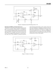
The AD628 can be operated as either a differential/
scaling amplier or as a pin-strapped precision gain
block. Specically designed for use ahead of an analog-
to-digital converter, the AD628 is extremely useful as an
input scaling and buffering amplier. As a differential
amplier, it can extract small differential voltages riding
on large common-mode voltages up to ±120 V. As a
prepackaged precision gain block, the pins of the AD628
can be strapped to provide a wide range of precision
gains, allowing for high accuracy data acquisition with
very little gain or offset drift.
The AD628 uses an absolute minimum of external com-
ponents. Its tiny MSOP provides these functions in the
smallest size package available in the market. Besides
high gain accuracy and low drift, the AD628 provides a
very high common-mode rejection, typically more than
90 dB at 1 kHz while still maintaining a 60 dB CMRR at
100 kHz.
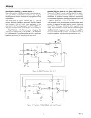
The AD628 includes a V
REF
pin to allow a dc (midscale)
offset for driving single-supply ADCs. In this case, the
V
REF
pin may simply be tied to the ADC’s reference pin,
which also allows easy ratio-metric operation.
Why Use a Gain Block IC?
Real-world measurement requires extracting weak
signals from noisy sources. Even when a differential
measurement is made, high common-mode voltages
are often present. The usual solution is to use an op amp
or, better still, an in amp, and then perform some type of
low-pass ltering to reduce the background noise level.
The problem with this traditional approach is that a
discrete op amp circuit will have poor common-mode
rejection and its input voltage range will always be less
than the power supply voltage. When used with a differ-
ential signal source, an in amp circuit using a monolithic
IC will improve common-mode rejection. However, signal
sources greater than the power supply voltage or signals
riding on high common-mode voltages can't handle stan-
dard in amps. In addition, in amps using a single external
gain resistor suffer from gain drift. Finally, low-pass l-
tering usually requires the addition of a separate op amp,
along with several external components. This drains valu-
able board space.
The AD628 eliminates these common problems by func-
tioning as a scaling amplier between the sensor, the
shunt resistor, or other point of data acquisition, as well
as the ADC. Its 120 V max input range permits the direct
measurement of large signals, or small signals riding on
large common-mode voltages.
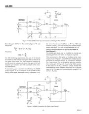
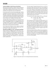
Standard Differential Input ADC Buffer Circuit with
Single-Pole LP Filter
Figure 1 shows the AD628 connected to accept a differ-
ential input signal riding on a very high common-mode
voltage. The AD628 gain block has two internal ampli-
fiers: A1 and A2. Pin 3 is grounded, thus operating
amplier A1 at a gain of 0.1. The 100 k input resistors
and other aspects of its design allow the AD628 to
process small input signals riding on common-mode
voltages up to ±120 V.
The output of A1 connects to the plus input of amplier
A2 through a 10 k resistor. Pin 4 allows connecting an
external capacitor to this point, providing single-pole
low-pass ltering.
Changing the Output Scale Factor
Figure 1 reveals that the output scale factor of the AD628
may be set by changing the gain of amplier A2. This
uncommitted op amp may be operated at any convenient
gain higher than unity. When congured, the AD628 may
be set to provide circuit gains between 0.1 and 1000.
REV. 0
器件 Datasheet 文档搜索
AiEMA 数据库涵盖高达 72,405,303 个元件的数据手册,每天更新 5,000 多个 PDF 文件
