Datasheet 搜索 > AD转换器 > TI(德州仪器) > ADS8327IBRSAR 数据手册 > ADS8327IBRSAR 开发手册 4/8 页
 器件3D模型
¥ 35.334
ADS8327IBRSAR 开发手册 - TI(德州仪器)
制造商:
TI(德州仪器)
分类:
AD转换器
封装:
VQFN-16
描述:
低功耗, 16位, 500千赫,单/双单极性输入,模拟 - 数字转换器,串行接口 LOW POWER, 16-BIT, 500-kHz, SINGLE/DUAL UNIPOLAR INPUT, ANALOG-TO-DIGITAL CONVERTERS WITH SERIAL INTERFACE
Pictures:
3D模型
符号图
焊盘图
引脚图
产品图
页面导航:
应用领域在P8
导航目录
ADS8327IBRSAR数据手册
Page:
of 8 Go
若手册格式错乱,请下载阅览PDF原文件
www.ti.com
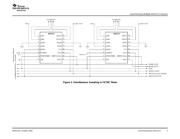
SYNC BEGINS
CLK
SYNC
CONVERSION
OLD CYCLE INTERRUPTED
DRDY
FIRST SAMPLE TAKEN
38 x T
S
or 39 x T
S
PREVIOUSLY
SETTLING: 128 x T
S
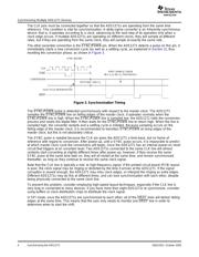
Synchronizing Multiple ADS1271 Devices
The CLK pins must be connected together so that the ADS1271s are operating from the same time
reference. This condition is vital for synchronization. A delta-sigma converter is an inherently synchronous
device: that is, it operates according to a clock, advancing to the next step of its operation only when a
clock edge occurs. If multiple ADS1271s are operating on different clocks, they will sample at different
rates; but if they are operating from the same clock, they will sample at exactly the same rate.
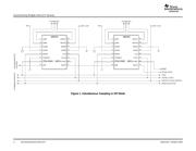
The other essential connection is the SYNC/ PDWN pin. When the ADS1271 detects a pulse on this pin, it
immediately starts a new conversion cycle (as well as a settling cycle, as explained in Section 2 ), thus
resetting the conversion phase, as shown in Figure 3 .
Figure 3. Synchronization Timing
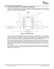
The SYNC/ PDWN pulse is detected synchronously with respect to the master clock. The ADS1271
samples the SYNC/ PDWN line on falling edges of the master clock. It operates normally when the
SYNC/ PDWN line is high. When the SYNC/ PDWN line is sampled low, the ADS1271 halts the conversion
process and resets the digital filter. It then waits for the SYNC/ PDWN line to return high. When the line is
sampled high, the converter restarts and a settling cycle is initiated. Because sampling occurs on the
falling edge of the master clock, it is recommended to transition SYNC/ PDWN at rising edges of the
master clock, but this is not absolutely critical.
The SYNC pulse is needed because the CLK pin gives the ADS1271 a time-base, but no frame of
reference with regard to conversion. After power-up, until a SYNC pulse occurs, it is impossible to predict
at which master clock cycle the conversions will begin, since the ADS1271 has an internal power-on reset
circuit that triggers at an uncertain level. Two ADS1271s connected to the same CLK line will almost
certainly start converting at slightly different times after power-up; however, if they receive the same
SYNC pulse at the same time later on, they will all restart at the same time, and remain synchronized
thereafter, as long as they continue to receive the same clock signal.
Note that the CLK line is typically a mid- to high-frequency signal. If the printed circuit board (PCB) layout
is poor, the clock signal may be ringing or distorted by the time it arrives at the ADS1271. If the signal
corruption is severe enough, the ADS1271 may miss clock edges, or interpret the ringing as extra edges.
Different ADS1271s may do this at different times, and can lose synchronization with each other, despite
being physically connected to the same clock line.
To prevent this problem, consider employing high-speed layout techniques, especially if the CLK line is
very long or connected to many devices. If you have more than eight ADS1271s to synchronize, consider
using buffers or clock distribution chips to distribute the clock signal.
In SPI mode, once the ADS1271s are synchronized to each other, all of the DRDY lines will deliver falling
edges at the same time. This means that the user only needs to monitor one DRDY line in order to
determine when to start the shift.
Synchronizing the ADS12714 SBAS355 – October 2005
器件 Datasheet 文档搜索
AiEMA 数据库涵盖高达 72,405,303 个元件的数据手册,每天更新 5,000 多个 PDF 文件
