Datasheet 搜索 > 接口隔离器 > ADI(亚德诺) > ADUM1301ARWZ 数据手册 > ADUM1301ARWZ 开发手册 3/8 页
 器件3D模型
¥ 14.59
ADUM1301ARWZ 开发手册 - ADI(亚德诺)
制造商:
ADI(亚德诺)
分类:
接口隔离器
封装:
SOIC-16
描述:
ANALOG DEVICES ADUM1301ARWZ 数字隔离器, 3通道, 100 ns, 2.7 V, 5.5 V, SOIC, 16 引脚
Pictures:
3D模型
符号图
焊盘图
引脚图
产品图
页面导航:
原理图在P4


导航目录
ADUM1301ARWZ数据手册
Page:
of 8 Go
若手册格式错乱,请下载阅览PDF原文件
AN-913
Rev. 0 | Page 3 of 8
Table 1. I
2
C Logic Levels
Parameter Symbol Min Max Unit Comments
Logic Low Input Voltage V
IL
−0.5 0.3 × V
DD
V
Standard mode allows for a fixed-input
specification (−0.5 V min, +1.5 V max)
Logic High Input Voltage V
IH
0.7 × V
DD
V
DD
+ 0.5 V
Logic Low Output Voltage (for 3 mA sink current)
V
DD
> 2 V V
OL1
0 0.4 V
V
DD
< 2 V V
OL3
0 0.2 × V
DD
V Standard mode does not allow for V
DD
< 2 V
Data transfer can occur at up to either 100 kbps (standard mode),
400 kbps (fast mode), 1 Mbps (fast mode plus), or 3.4 Mbps
(high speed mode). There is no limit to the number of devices
that can be connected to the bus—as long as a 400 pF bus limit
is not exceeded. The logic levels for I
2
C are shown in Tabl e 1 .
An important aspect of the I
2
C interface is that SDA logic
transitions can only occur while the SCL clock signal is low.
Also, the start and stop signals that bound the transmittal of
data are SDA logic transitions that occur while the SCL clock
signal is high. Therefore, it is important that the SCL signal be
stable in both its low and high states to avoid communication
problems on the bus.
THE CHALLENGE OF ISOLATED I
2
C INTERFACES
The bidirectional nature of the I
2
C interface presents special
challenges in implementing isolation in a manner that avoids
bus glitches or lock-up.
Figure 2 shows a circuit based on
optocoupler technology. Since optocouplers are inherently
unidirectional devices, each bidirectional I
2
C line must be
broken out into two unidirectional lines to support commu-
nication through the optocouplers. In
Figure 2, only the SDA
lines are shown for simplicity. Isolating a complete I
2
C interface
requires four optocouplers. The resulting increase in cost, board
space, and complexity diminishes the inherent value (that of
providing a simple, low cost, 2-wire interface) of I
2
C.
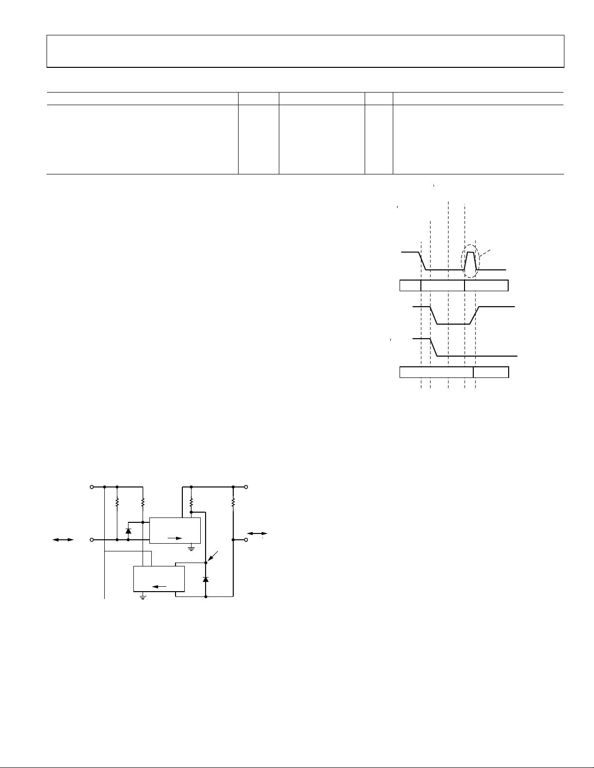
06751-002
R
1
3.3kΩ
R
2
2.2kΩ
R
3
2.2kΩ
R
4
3.3kΩ
D
1
OCTOCOUPLER
IC
1
OCTOCOUPLER
IC
2
D
2
NODE1
5V 5V
SDA
MASTER
SDA
SLAVE
Figure 2. An Optocoupler-Based I
2
C interface
06751-003
SDA
SDA
BUS GLITCH
SDA TAKEN
LOW BY MASTER
SDA PULLED LOW
VIA OPTOCOUPLER IC
1
SDA TAKEN
LOW BY SLAVE
SDA RELEASED
BY MASTER
SDA RECOVERS
TO LOW STATE
AFER OPTOCOUPLER
PROPAGATION DELAYS
NODE1
OPTOCOUPLER IC
2
OPTOCOUPLER IC
1
OFF
OFF OFF
ON
ON
Figure 3. Optocoupler-based I
2
C Interface Waveforms
An additional problem with a circuit such as this is that it
results in undesirable bus glitches (see
Figure 3).
• A high-to-low transition occurs at SDA. In this situation,
IC
1
is turned on by the current flowing through R
2
. This,
in turn, pulls Node 1 low and consequently pulls SDA'
low via D
2
.
• SDA' is taken low. Nothing changes except D
2
no longer
conducts.
• SDA is released and goes high as there is nothing holding it
low. The LED in IC
1
turns off. After a delay, the transistors
of IC
1
turn off. Node 1 goes high and turns on the LED in
IC
2
. After another delay, the transistors of IC
2
turn on and
SDA is pulled low to the desired state.
Notice that SDA is high for the duration it takes for IC
1
to turn
off and IC
2
to turn on. This is an unwanted glitch on the bus in
which SDA is high while SDA' is trying to bring the bus low.
器件 Datasheet 文档搜索
AiEMA 数据库涵盖高达 72,405,303 个元件的数据手册,每天更新 5,000 多个 PDF 文件
