Datasheet 搜索 > 多工器 > Maxim Integrated(美信) > MAX4899AEETE+T 数据手册 > MAX4899AEETE+T 开发手册 1/13 页
 器件3D模型
¥ 31.414
MAX4899AEETE+T 开发手册 - Maxim Integrated(美信)
制造商:
Maxim Integrated(美信)
分类:
多工器
封装:
TQFN-16
描述:
MAXIM INTEGRATED PRODUCTS MAX4899AEETE+T 芯片, 模拟多路复用器, 双路, 4:1, TQFN-16
Pictures:
3D模型
符号图
焊盘图
引脚图
产品图
页面导航:
原理图在P10
应用领域在P5P9P11P12
导航目录
MAX4899AEETE+T数据手册
Page:
of 13 Go
若手册格式错乱,请下载阅览PDF原文件
Maxim > Design Support > Technical Documents > Application Notes > Analog Switches and Multiplexers > APP 5299
Keywords: CMOS, analog switch, MUX, multiplexers, on-resistance, RON flatness, THD, charge injection, off-isolation, ESD protection, fault-protection, force-sense switches, leakage current, video
switch, high-speed USB, HDMI, PCIe, high voltage switch
APPLICATION NOTE 5299
Selecting the Right CMOS Analog Switch
By: Usama Munir, Application Engineer
David Canny, Application Engineer
Jan 29, 2013
Abstract:
With the large number
of analog switches on the market today, there are many performance criteria for a product designer to consider. This application note reviews the basic construction of
the standard CMOS analog switch and describes some common analog-switch parameters. It also discusses the improved performance offered by the latest analog switches.
A similar version of this article appears in German in two parts on Elektronikpraxis, November 27, 2012 and December 4, 2012.
Introduction
Integrated analog switches often form the interface between analog signals and a digital controller. With the large number of analog switches on the market today, there are many performance criteria
for a product designer to consider. There are also many application-specific switch circuits that have evolved from the standard CMOS switch developed over 35 years ago.
This article reviews the basic construction of the standard CMOS analog switch and describes some common analog-switch parameters such as on-resistance (R
ON
), R
ON
flatness, leakage, charge
injection, and off-isolation. It discusses the improved performance offered by the latest analog switches: better switching characteristics, lower supply voltages, and smaller packages. Application-
specific features such as fault protection, ESD protection, calibration multiplexers (cal-muxes), and force-sense capability are explained. Application-specific switches for video, Hi-Speed USB, HDMI
®
,
and PCIe
®
applications are presented.
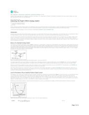
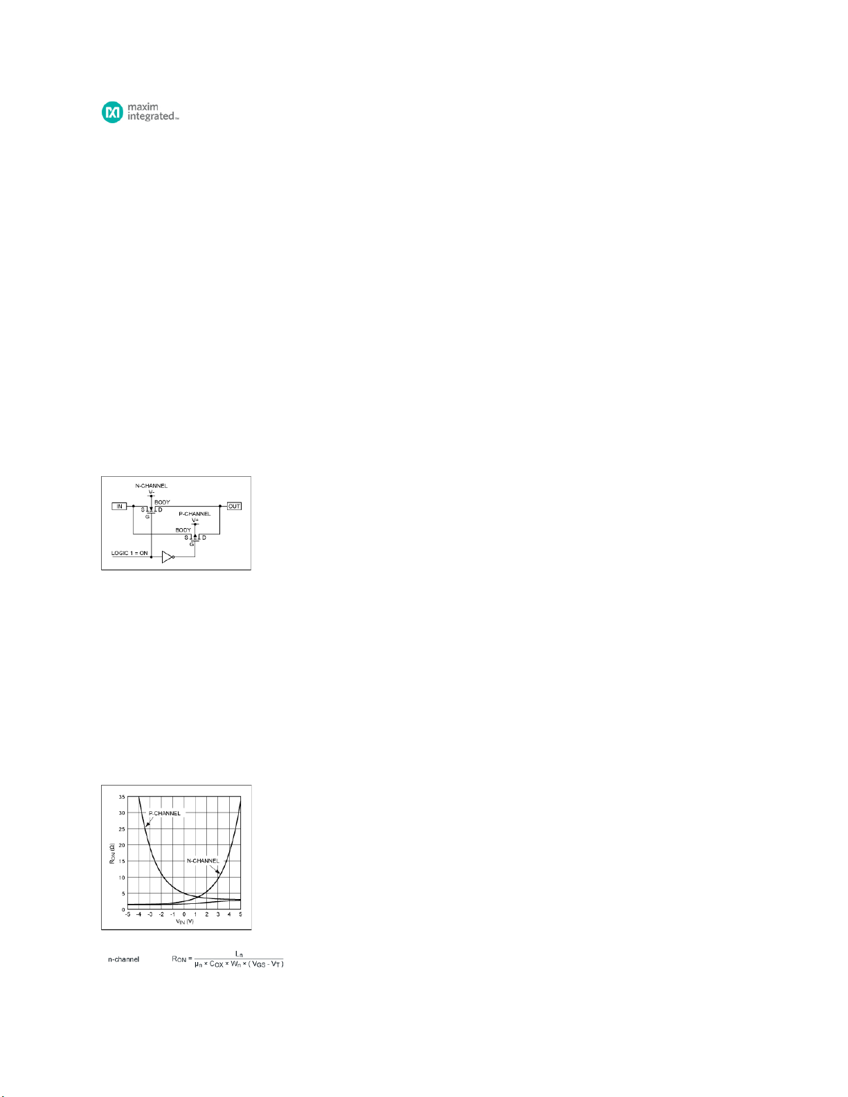
Basics of a Standard Analog Switch
The structure of a conventional analog switch is shown in Figure 1. Connecting an n-channel MOSFET in parallel with a p-channel MOSFET allows signals to pass in either direction with equal ease.
The n-channel device carries signal current that is dependent on the ratio of input voltage to positive supply voltage, while the p-channel device carries signal current that is dependent on the ratio of
input voltage to negative supply voltage (or ground in single-supply designs). Because the switch has no preferred direction for current flow, it has no preferred input or output. The two MOSFETs are
switched on and off by internal inverting and noninverting amplifiers. These amplifiers level shift the digital input signal as required, according to whether the signal is CMOS- or TTL-logic compatible
and whether the analog supply voltage is a single or dual supply.
Figure 1. The internal construction of a typical analog switch features parallel n- and p-channel MOSFETs.
Conventional analog switches like the early CD4066 are now offered by many semiconductor manufacturers. Maxim also offers devices such as the MAX4610, which is pin-for-pin compatible with
these earlier switches, but provides better performance. For example, there are now CD4066 pin-for-pin compatible parts that provide lower R
ON
and higher accuracy than the original CD4066.
There are also some functional variations to the basic analog switch construction. Some low-capacitance analog switches use only n-channel MOSFETs in the signal path (e.g., the MAX4887) and
eliminate the larger p-channel MOSFETs that significantly reduce the bandwidth of the analog switch.
Other analog switches operating from a single positive supply rail use charge pumps to allow negative signal voltages. For example, the MAX14504 audio switch operates from a single +2.3V
CC
to
+5.5V
CC
supply and an internal charge pump allows signal capability from -V
CC
to +V
CC
to pass without distortion. In addition to improved functionality, many of the industry's latest analog switches
are offered in smaller packages than earlier generation parts.
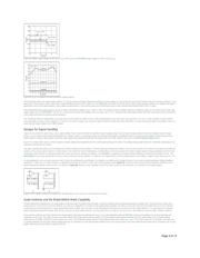
Low On-Resistance (R
ON
) Switches Reduce Signal Losses
The combined p- and n-channel R
ON
in parallel for each level of V
IN
yields a composite R
ON
characteristic for the parallel structure (Figure 2). This plot of R
ON
versus V
IN
can be described as linear
if you exclude the effects of temperature, power-supply voltage, and R
ON
variation with analog input voltage. Ideally, R
ON
would be as low as possible in order to keep the signal losses and
propagation delays small. However, reducing R
ON
involves increasing the width/length (W/L) ratio of a MOSFET's silicon, which results in higher parasitic capacitance and a larger silicon area. This
larger parasitic capacitance reduces the bandwidth of the analog switch. Apart from W and L, R
ON
is a complex function of electron and hole mobility (µ
n
and µ
p
), oxide capacitance (C
OX
), threshold
voltage (V
T
), and signal voltage, V
GS
(V
IN
), of the n- and p-MOSFETs as shown in Equations 1a and 1b below.
Minimizing R
ON
and the parasitic capacitance, along with improving the linearity of R
ON
versus V
IN
over temperature and voltages, are often the primary purposes for designing new products.
Figure 2. R
ON
versus V
IN
. The n-channel and p-channel R
ON
of Figure 1 form a low-valued composite R
ON
.
(Eq. 1a)
Page 1 of 13
器件 Datasheet 文档搜索
AiEMA 数据库涵盖高达 72,405,303 个元件的数据手册,每天更新 5,000 多个 PDF 文件
