Datasheet 搜索 > 多工器 > Maxim Integrated(美信) > MAX4899AEETE+T 数据手册 > MAX4899AEETE+T 开发手册 5/13 页
 器件3D模型
¥ 31.38
MAX4899AEETE+T 开发手册 - Maxim Integrated(美信)
制造商:
Maxim Integrated(美信)
分类:
多工器
封装:
TQFN-16
描述:
MAXIM INTEGRATED PRODUCTS MAX4899AEETE+T 芯片, 模拟多路复用器, 双路, 4:1, TQFN-16
Pictures:
3D模型
符号图
焊盘图
引脚图
产品图
页面导航:
原理图在P10
应用领域在P5P9P11P12
导航目录
MAX4899AEETE+T数据手册
Page:
of 13 Go
若手册格式错乱,请下载阅览PDF原文件
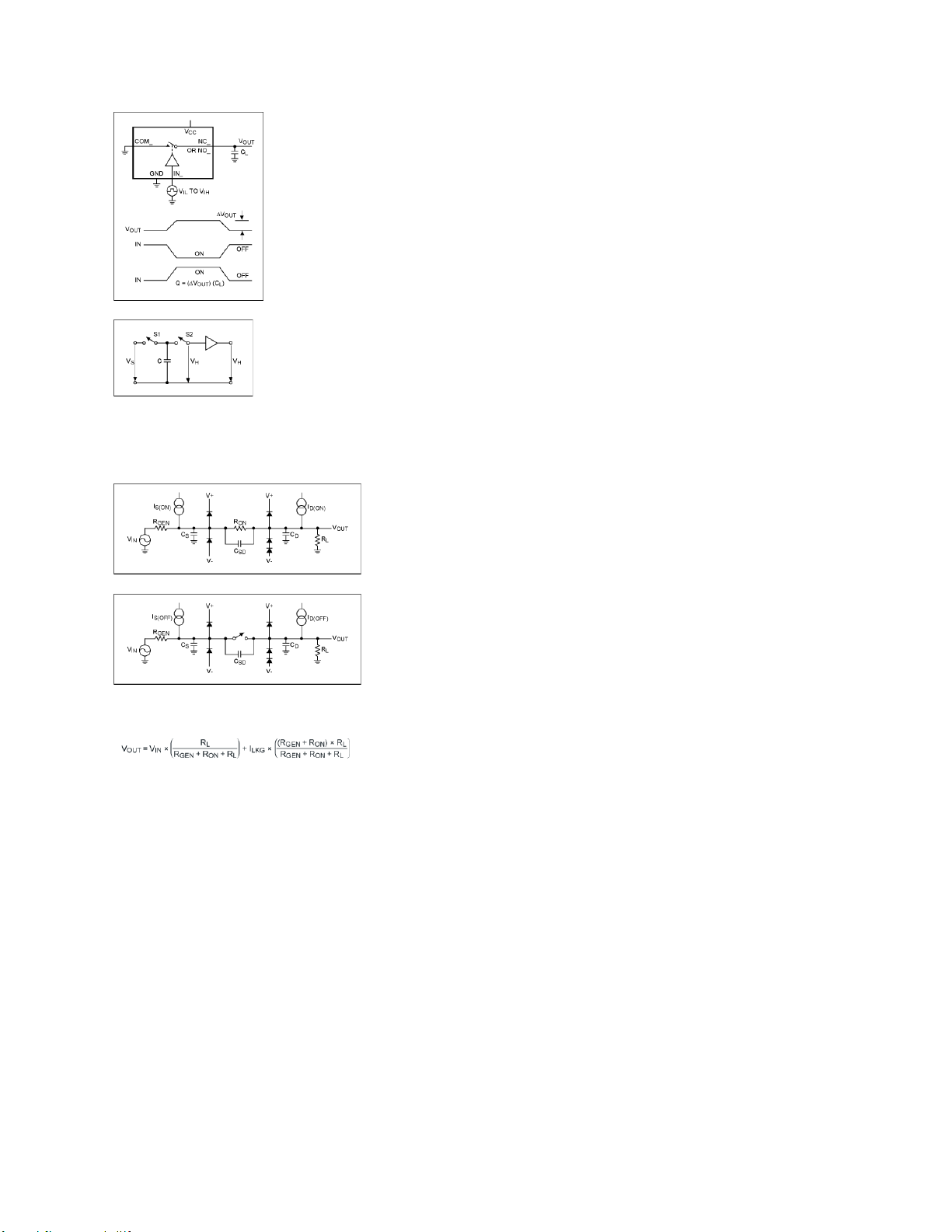
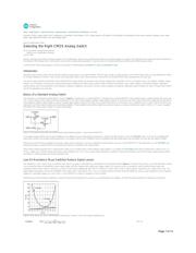
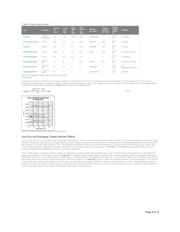
Figure 6A. Charge injection from the switch-control signal causes a voltage error at the analog output.
Figure 6B. A typical track-and-hold function in an ADC requires precise control of the analog switches.
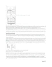
Leakage Currents and Their Impact on Voltage Error
Leakage current affects the output voltage of an analog switch. Figures 7 and 8 show the simplified small-signal models of an analog switch in the on and off states. In both cases, most of the
leakage current flows through the internal parasitic diodes, and this contributes to the output voltage error. The leakage current is also a function of temperature and doubles approximately every 10°C.
ESD protection diodes (e.g., in fault-protected switches) increase the leakage currents.
Figure 7. Equivalent circuit diagram for a closed switch.
Figure 8. Equivalent circuit diagram for an open switch.
The output voltage for the on-state is calculated in Equation 3 and is a function of leakage current, R
ON
, R
ON
variation over the applied input signal, load resistance, and source resistance. For
bidirectional analog switches I
LKG
is equal to I
S
or I
D
(shown in Figures 7 and 8) depending on whether the drain or source side of the switch is configured as the output.
(Eq. 3)
The output voltage for the off-state is principally affected by leakage current and is calculated by V
OUT
= I
LKG
× R
L
.
Many IC data sheets specify on/off leakage currents for worst-case scenarios: When the signal voltage approaches the supply voltage limits, this causes the parasitic diodes to inject higher currents
into the substrate and results in current flow into adjacent channels. Consequently, a designer should be aware of the supply currents' absolute maximum rating for the part being used and should not
exceed these limits. Exceeding the limits can permanently damage a device. Applications with operational amplifiers or ADCs that switch high-input impedances and require low-offset errors should
use analog switches and multiplexers with low leakage currents.
Special Needs for Video and High-Frequency Switches
The trade-off between R
ON
and parasitic capacitance is important for video signals. Traditional analog switches with large R
ON
can require extra gain stages to compensate for the insertion loss.
Meanwhile, low R
ON
switches have larger parasitic capacitance that reduces bandwidth and degrades the video quality. Low R
ON
switches require input buffers to preserve the bandwidth, but this
increases the component count.
Employing only n-channel switches improves bandwidth, as parasitic components and package size become smaller and allow, in turn, more switches per unit area. However, n-channel switches suffer
from limited rail-to-rail operation. When an applied video signal exceeds these limits, the output clamps and the video signal is distorted. When selecting an n-channel switch, ensure that the specified
limits of the switch are sufficient for passing through the full input-signal range.
In applications where a monitor displays video from many sources as in a security and surveillance system, off-isolation and crosstalk are key parameters. With a switch in the off state, the amount of
feedthrough from an applied input signal determines the off-isolation. At high frequencies, which are typical in video and VHF applications, the signal is coupled through the drain-to-source capacitance
(C
DS
) that reduces off-isolation. The higher circuit impedances associated with the switch also contribute to reducing off-isolation.
The T-switch topology is suitable for video and other frequencies above 10MHz. It consists of two analog switches in series, with a third switch connected between their common connection and
ground (Figure 9A). This arrangement provides higher off-isolation than a single switch. The capacitive crosstalk for a T switch that is turned off typically rises with frequency because of the parasitic
capacitances in parallel with each of the series switches (Figure 9A). In multiple-channel switches, the parasitic capacitances between channels capacitively couples the signal into the adjacent
channels, thereby increasing crosstalk.
When the T-switch in Figure 9A is turned on, S1 and S2 are closed and S3 is open. In the off state, S1 and S2 are open and S3 is closed. In this off state the signal tries to couple through C
DS
of the
series MOSFETs, but it is shunted to ground by S3. The difference between off-isolation at 10MHz for a video T-switch (e.g., the MAX4545) and a standard analog switch (e.g., the MAX312) is
dramatic: -80dB versus -36dB (Figure 9B).
Page 5 of 13
器件 Datasheet 文档搜索
AiEMA 数据库涵盖高达 72,405,303 个元件的数据手册,每天更新 5,000 多个 PDF 文件
