Datasheet 搜索 > 逻辑芯片 > ON Semiconductor(安森美) > MC14049UBDG 数据手册 > MC14049UBDG 开发手册 1/2 页
 器件3D模型
¥ 2.889
MC14049UBDG 开发手册 - ON Semiconductor(安森美)
制造商:
ON Semiconductor(安森美)
分类:
逻辑芯片
封装:
SOIC-16
描述:
ON SEMICONDUCTOR MC14049UBDG. 芯片, 反相缓冲器, SOIC-16
Pictures:
3D模型
符号图
焊盘图
引脚图
产品图
页面导航:
型号编码规则在P2
应用领域在P1
导航目录
MC14049UBDG数据手册
Page:
of 2 Go
若手册格式错乱,请下载阅览PDF原文件
Semiconductor Components Industries, LLC, 2003
November, 2003 − Rev. 3
1 Publication Order Number:
AND8053/D
AND8053/D
Designing Crystal
Oscillators with Modern
CMOS Gates
Prepared by: Fred Zlotnick
Applications Manager
INTRODUCTION
Designing a crystal oscillator with modern CMOS gates
is difficult with the limited information available. The
designer has many families to choose from: 4000 series,
HCMOS, LCX, and VHC, for starters. The selection of the
logic family depends on the system voltage and frequency
of operation.
Designing a crystal oscillator using gates instead of
buying a pre−packaged device that includes all the active
components provides the following benefits:
• Save Money
• Control the Parameters that are Critical to the Design
In order to save money, the designer has to be willing to
undertake the design and understand the tradeoffs. By doing
this, he also is able to take control of critical parameters such
as frequency, accuracy, and stability.
This article will only be concerned with the fundamental
mode operation. Today’s crystals can be purchased with
fundamental modes up to about 30 MHz. These techniques
also work well for ceramic resonators.
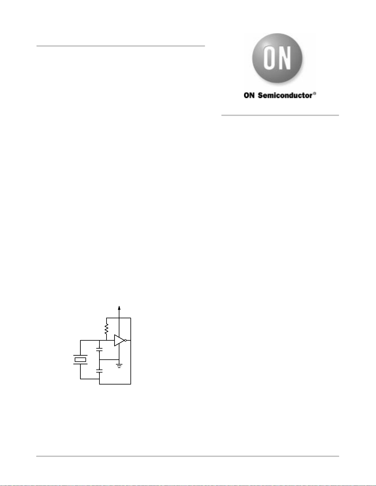
V
CC
Figure 1. Crystal Oscillator Using
Unbuffered CMOS Gate
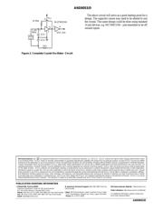
Theory of operation: in nearly all cases, using a gate as an
oscillator entails causing the gate to go into class “A” or
biased between the on and off state. This is accomplished by
placing a large resistor, between 10 and 20 M from the
output to the input. The mode of operation is the “Pierce”
crystal oscillator (Amateur Radio Handbook, 1968).
This circuit can be considered a grounded source
transistor, with Capacitors to ground. The input (gate) and
output (drain) are “floating.” This circuit has been around in
vacuum tube form for many years, and is just a modern
version of the circuit. To implement this circuit, an
“unbuffered” inverter is usually used (see Figure 1). Devices
such as the MC74VHCU04 or MC74LCXU04, available
from ON Semiconductor, will provide stable operation from
below 1 MHz to above 20 MHz, from 2−5 volts operation.
Since there are six active inverters in each 14−pin package,
the designer is encouraged to use at least one of the devices
as a buffer. The unbuffered gate, such as a VHCU04,
contains just one P−Channel, and one N−Channel device.
Since there is just one complementary pair, this is only one
transistor gate delay. These devices are fabricated in 0.6
CMOS and have significant Class A gain for any crystal
application up to 100 MHz or more. If the designer needs a
circuit to operate between 7 and 18 volts, the MC14049UB
from the 4000 series of Metal Gate CMOS makes a good
choice. The designer has to be careful not to make demands
on the circuit that exceed the maximum frequency
capabilities of this family (~ 4−10 MHz).
In all cases, the designer needs to be aware that it is
possible to damage the crystal with over−active excitation.
By using the unbuffered inverters and a series resistor (see
Figure 2), in the VHC or Metal gate series, the designer can
be confident that there will not be too much drive. A test to
determine whether appropriate drive is being obtained is
described in the High−Speed CMOS Data book, DL129/D.
The designer builds a prototype of the circuit and applies
V
CC
through a variable supply. If the frequency shifts very
slightly higher when the supply voltage is varied, the design
is valid. If the frequency decreases or becomes unstable, a
resistor should be added to the circuit.
APPLICATION NOTE
http://onsemi.com
器件 Datasheet 文档搜索
AiEMA 数据库涵盖高达 72,405,303 个元件的数据手册,每天更新 5,000 多个 PDF 文件
