Datasheet 搜索 > DC/DC转换器 > ON Semiconductor(安森美) > MC34063ADR2G 数据手册 > MC34063ADR2G 开发手册 1/43 页
 器件3D模型
¥ 2.07
MC34063ADR2G 开发手册 - ON Semiconductor(安森美)
制造商:
ON Semiconductor(安森美)
分类:
DC/DC转换器
封装:
SOIC-8
描述:
ON Semiconductor
Pictures:
3D模型
符号图
焊盘图
引脚图
产品图
页面导航:
导航目录
MC34063ADR2G数据手册
Page:
of 43 Go
若手册格式错乱,请下载阅览PDF原文件
© Semiconductor Components Industries, LLC, 2013
December, 2013 − Rev. 6
1 Publication Order Number:
AN920/D
AN920/D
Theory and Applications
of the MC34063 and
mA78S40 Switching
Regulator Control Circuits
This paper describes in detail the principle of operation of the MC34063 and μA78S40 switching regulator subsystems. Several
converter design examples and numerous applications circuits with test data are included.
INTRODUCTION
The MC34063 and μA78S40 are monolithic switching
regulator subsystems intended for use as dc to dc converters.
These devices represent a significant advancement in the
ease of implementing highly efficient and yet simple
switching power supplies. The use of switching regulators
is becoming more pronounced over that of linear regulators
because the size reductions in new equipment designs
require greater conversion efficiency. Another major
advantage of the switching regulator is that it has increased
application flexibility of output voltage. The output can be
less than, greater than, or of opposite polarity to that of the
input voltage.
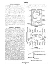
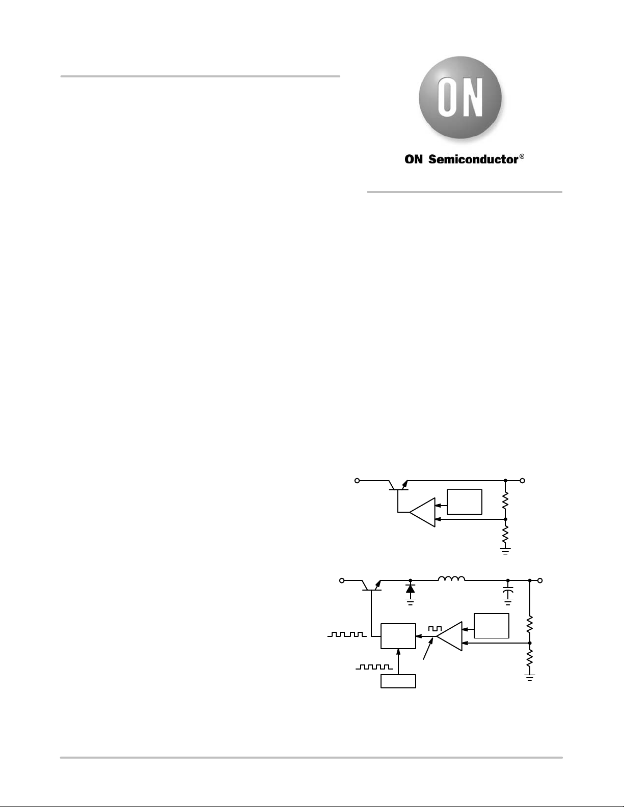
PRINCIPLE OF OPERATION
In order to understand the difference in operation between
linear and switching regulators we must compare the block
diagrams of the two step−down regulators shown in Figure
1. The linear regulator consists of a stable reference, a high
gain error amplifier, and a variable resistance series−pass
element. The error amplifier monitors the output voltage
level, compares it to the reference and generates a linear
control signal that varies between two extremes, saturation
and cutoff. This signal is used to vary the resistance of the
series−pass element in a corrective fashion in order to
maintain a constant output voltage under varying input
voltage and output load conditions.
The switching regulator consists of a stable reference and
a high gain error amplifier identical to that of the linear
regulator. This system differs in that a free running oscillator
and a gated latch have been added. The error amplifier again
monitors the output voltage, compares it to the reference
level and generates a control signal. If the output voltage is
below nominal, the control signal will go to a high state and
turn on the gate, thus allowing the oscillator clock pulses to
drive the series−pass element alternately from cutoff to
saturation. This will continue until the output voltage is
pumped up slightly above its nominal value. At this time, the
control signal will go low and turn off the gate, terminating
any further switching of the series−pass element. The output
voltage will eventually decrease to below nominal due to the
presence of an external load, and will initiate the switching
process again. The increase in conversion efficiency is
primarily due to the operation of the series−pass element
only in the saturated or cutoff state. The voltage drop across
the element, when saturated, is small as is the dissipation.
When in cutoff, the current through the element and likewise
the power dissipation are also small. There are other
variations of switching control. The most common are the
fixed frequency pulse width modulator and the fixed
on−time variable off−time types, where the on−off
switching is uninterrupted and regulation is achieved by
duty cycle control. Generally speaking, the example given
in Figure 1b does apply to MC34063 and μA78S40.
Figure 1. Step−Down Regulators
+
−
V
in
V
out
Ref
Voltage
Error
Amp
Linear Control
Signal
+
−
V
in
V
out
Ref
Voltage
Error
Amp
Digital
Control Signal
Gated
Latch
OSC
a. Linear Regulator
b. Switching Regulator
APPLICATION NOTE
http://onsemi.com
器件 Datasheet 文档搜索
AiEMA 数据库涵盖高达 72,405,303 个元件的数据手册,每天更新 5,000 多个 PDF 文件
