Datasheet 搜索 > DC/DC转换器 > ON Semiconductor(安森美) > MC34063ADR2G 数据手册 > MC34063ADR2G 开发手册 5/43 页
 器件3D模型
¥ 2.07
MC34063ADR2G 开发手册 - ON Semiconductor(安森美)
制造商:
ON Semiconductor(安森美)
分类:
DC/DC转换器
封装:
SOIC-8
描述:
ON Semiconductor
Pictures:
3D模型
符号图
焊盘图
引脚图
产品图
页面导航:
导航目录
MC34063ADR2G数据手册
Page:
of 43 Go
若手册格式错乱,请下载阅览PDF原文件

AN920/D
http://onsemi.com
5
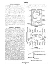
value. The output voltage across capacitor C
o
will
eventually decay below nominal because it is the only
component supply current into the external load R
L
. This
voltage deficiency is monitored by the switching control
circuit and causes it to drive Q1 into saturation. The inductor
current will start to flow from V
in
through Q1 and, C
o
in
parallel with R
L
, and rise at a rate of ΔI/ΔT = V/L. The
voltage across the inductor is equal to V
in
− V
sat
− V
out
and
the peak current at any instant is:
I
L
+
ǒ
V
in
* V
sat
* V
out
L
Ǔ
t
At the end of the on−time, Q1 is turned off. As the magnetic
field in the inductor starts to collapse, it generates a reverse
voltage that forward biases D1, and the peak current will
decay at a rate of ΔI/ΔT = V/L as energy is supplied to C
o
and
R
L
. The voltage across the inductor during this period is equal
to V
out
+ V
F
of D1, and the current at any instant is:
I
L
+ I
L(pk)
*
ǒ
V
out
) V
F
L
Ǔ
t
Assume that during quiescent operation the average
output voltage is constant and that the system is operating in
the discontinuous mode. Then I
L(peak)
attained during t
on
must decay to zero during t
off
and a ratio of t
on
to t
off
can be
determined.
ǒ
V
in
* V
sat
* V
out
L
Ǔ
t
on
+
ǒ
V
out
) V
F
L
Ǔ
t
off
N
t
on
t
off
+
V
out
) V
F
V
in
* V
sat
* V
out
Note that the volt−time product of t
on
must be equal to that
of t
off
and the inductance value is not of concern when
determining their ratio. If the output voltage is to remain
constant, the average current into the inductor must be equal
to the output current for a complete cycle. The peak inductor
current with respect to output current is:
ǒ
I
L(pk)
2
Ǔ
t
on
)
ǒ
I
L(pk)
2
Ǔ
t
off
+
ǒ
I
out
t
on
Ǔ
)
ǒ
I
out
t
off
Ǔ
NI
L(pk)
+ 2I
out
I
L(pk)
(t
on
) t
off
)
2
+ I
out
(t
on
) t
off
)
The peak inductor current is also equal to the peak switch
current I
pk(switch)
since the two are in series. The on−time, t
on
,
is the maximum possible switch conduction time. It is equal
to the time required for C
T
to ramp up from its lower to upper
threshold. The required value for C
T
can be determined by
using the minimum oscillator charging current and the
typical value for the oscillator voltage swing both taken
from the data sheet electrical characteristics table.
C
T
+ I
chg(min)
ǒ
Dt
DV
Ǔ
+ 20 10
− 6
ǒ
t
on
0.5
Ǔ
+ 4.0 10
− 5
t
on
The off−time, t
off
, is the time that diode D1 is in
conduction and it is determined by the time required for the
inductor current to return to zero. The off−time is not related
to the ramp−down time of C
T
. The cycle time of the LC
network is equal to t
on(max)
+ t
off
and the minimum operating
frequency is:
f
min
+
1
t
on(max)
) t
off
A minimum value of inductance can now be calculated for
L. The known quantities are the voltage across the inductor
and the required peak current for the selected switch
conduction time.
L
min
+
V
in
* V
sat
* V
out
I
pk(switch)
t
on
This minimum value of inductance was calculated by
assuming the onset of continuous conduction operation with
a fixed input voltage, maximum output current, and a
minimum charge−current oscillator.
The net charge per cycle delivered to the output filter
capacitor C
o
, must be zero, Q+ = Q−, if the output voltage
is to remain constant. The ripple voltage can be calculated
from the known values of on−time, off−time, peak inductor
current, and output capacitor value.
V
ripple(p−p)
+
ǒ
1
C
o
Ǔ
ŕ
t
1
0
itdt)
ǒ
1
C
o
Ǔ
ŕ
t
2
t
1
iȀ tdt
it+
1
2
I
pk
t
t
on
ń2
where and
iȀ t +
1
2
I
pk
t
t
off
ń2
+
1
C
o
Ť
I
pk
t
on
t
2
2
Ť
t
1
0
)
1
C
o
Ť
I
pk
t
off
t
2
2
Ť
t
2
t
1
t
1
+
t
on
2
And and
t
2
* t
1
+
t
off
2
Substituting for t
1
and t
2
− t
1
yields:
+
I
pk
(t
on
) t
off
)
8C
o
+
1
C
o
I
pk
t
on
(t
on
ń2)
2
2
)
1
C
o
I
pk
t
off
(t
off
ń2)
2
2
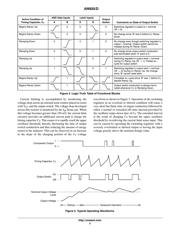
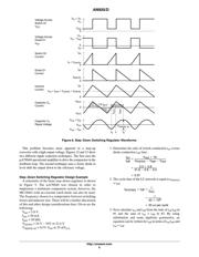
A graphical derivation of the peak−to−peak ripple voltage
can be obtained from the capacitor current and voltage
waveforms in Figure 8.
The calculations shown account for the ripple voltage
contributed by the ripple current into an ideal capacitor. In
practice, the calculated value will need to be increased due to
the internal equivalent series resistance ESR of the capacitor.
The additional ripple voltage will be equal to I
pk
(ESR).
Increasing the value of the filter capacitor will reduce the
output ripple voltage. However, a point of diminishing return
will be reached because the comparator requires a finite
voltage difference across its inputs to control the latch. This
voltage difference to completely change the latch states is
about 1.5 mV and the minimum achievable ripple at the output
will be the feedback divider ratio multiplied by 1.5 mV or:
V
ripple(p−p)min
+
V
out
V
ref
(1.5 10
− 3
)
器件 Datasheet 文档搜索
AiEMA 数据库涵盖高达 72,405,303 个元件的数据手册,每天更新 5,000 多个 PDF 文件
