Datasheet 搜索 > FET驱动器 > ST Microelectronics(意法半导体) > VN7050AJTR 数据手册 > VN7050AJTR 开发手册 5/55 页

¥ 5.237
VN7050AJTR 开发手册 - ST Microelectronics(意法半导体)
制造商:
ST Microelectronics(意法半导体)
分类:
FET驱动器
封装:
PowerSSO-16
描述:
VN7050AJ 系列 28 V 50 mOhm 高边 驱动器 带多路检测 模拟反馈
Pictures:
3D模型
符号图
焊盘图
引脚图
产品图
页面导航:
引脚图在P7Hot
原理图在P7P8
封装尺寸在P44P45P46P47P48P49P50P51P52
标记信息在P51P52
封装信息在P47P49P53
技术参数、封装参数在P9
应用领域在P1
电气规格在P9P10P11P12P13P14P15P16P17P18P19P20

导航目录
VN7050AJTR数据手册
Page:
of 55 Go
若手册格式错乱,请下载阅览PDF原文件

VN7050AJ, VN7050AS
List of figures
List of figures
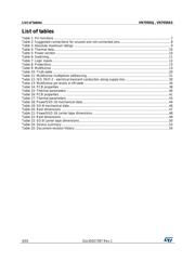
Figure 1: Block diagram .............................................................................................................................. 7
Figure 2: Configuration diagram (top view)................................................................................................. 8
Figure 3: Current and voltage conventions ................................................................................................. 9
Figure 4: IOUT/ISENSE versus IOUT ....................................................................................................... 17
Figure 5: Current sense accuracy versus IOUT ....................................................................................... 18
Figure 6: Switching time and Pulse skew ................................................................................................. 18
Figure 7: MultiSense timings (current sense mode) ................................................................................. 19
Figure 8: Multisense timings (chip temperature and VCC sense mode) (VN7050AJ only) ...................... 19
Figure 9: TDSTKON .................................................................................................................................. 20
Figure 10: Latch functionality - behavior in hard short circuit condition (TAMB << TTSD) ...................... 21
Figure 11: Latch functionality - behavior in hard short circuit condition .................................................... 22
Figure 12: Latch functionality - behavior in hard short circuit condition (autorestart mode + latch off) .... 22
Figure 13: Standby mode activation ......................................................................................................... 23
Figure 14: Standby state diagram ............................................................................................................. 23
Figure 15: OFF-state output current ......................................................................................................... 24
Figure 16: Standby current ....................................................................................................................... 24
Figure 17: IGND(ON) vs. Tcase ............................................................................................................... 24
Figure 18: Logic Input high level voltage .................................................................................................. 24
Figure 19: Logic Input low level voltage.................................................................................................... 24
Figure 20: High level logic input current ................................................................................................... 24
Figure 21: Low level logic input current .................................................................................................... 25
Figure 22: Logic Input hysteresis voltage ................................................................................................. 25
Figure 23: FaultRST Input clamp voltage ................................................................................................. 25
Figure 24: Undervoltage shutdown ........................................................................................................... 25
Figure 25: On-state resistance vs. Tcase ................................................................................................. 25
Figure 26: On-state resistance vs. VCC ................................................................................................... 25
Figure 27: Turn-on voltage slope .............................................................................................................. 26
Figure 28: Turn-off voltage slope .............................................................................................................. 26
Figure 29: Won vs. Tcase ......................................................................................................................... 26
Figure 30: Woff vs. Tcase ......................................................................................................................... 26
Figure 31: ILIMH vs. Tcase ....................................................................................................................... 26
Figure 32: OFF-state open-load voltage detection threshold ................................................................... 26
Figure 33: Vsense clamp vs. Tcase .......................................................................................................... 27
Figure 34: Vsenseh vs. Tcase .................................................................................................................. 27
Figure 35: Application diagram ................................................................................................................. 29
Figure 36: Simplified internal structure ..................................................................................................... 29
Figure 37: MultiSense and diagnostic – block diagram ............................................................................ 31
Figure 38: MultiSense block diagram ....................................................................................................... 32
Figure 39: Analogue HSD – open-load detection in off-state ................................................................... 33
Figure 40: Open-load / short to VCC condition ......................................................................................... 34
Figure 41: GND voltage shift .................................................................................................................... 35
Figure 42: Maximum turn off current versus inductance .......................................................................... 37
Figure 43: PowerSSO-16 on two-layers PCB (2s0p to JEDEC JESD 51-5) ............................................ 38
Figure 44: PowerSSO-16 on four-layers PCB (2s2p to JEDEC JESD 51-7) ........................................... 38
Figure 45: PowerSSO-16 Rthj-amb vs PCB copper area in open box free air condition (one channel on)
.................................................................................................................................................................. 39
Figure 46: PowerSSO-16 thermal impedance junction ambient single pulse (one channel on) .............. 39
Figure 47: Thermal fitting model of a double-channel HSD in PowerSSO-16.......................................... 40
Figure 48: S0-8 on two-layers PCB (2s0p to JEDEC JESD 51-5) ........................................................... 41
Figure 49: SO-8 on four-layers PCB (2s2p to JEDEC JESD 51-7) .......................................................... 41
Figure 50: SO-8 Rthj-amb vs PCB copper area in open box free air condition (one channel on) ........... 42
Figure 51: SO-8 thermal impedance junction ambient single pulse (one channel on) ............................. 42
Figure 52: Thermal fitting model of a double-channel HSD in SO-8 ........................................................ 43
DocID027397 Rev 1 5/55
器件 Datasheet 文档搜索
AiEMA 数据库涵盖高达 72,405,303 个元件的数据手册,每天更新 5,000 多个 PDF 文件
