Datasheet 搜索 > EEPROM芯片 > Microchip(微芯) > 24LC01B/SN 数据手册 > 24LC01B/SN 数据手册 3/34 页
 器件3D模型
¥ 2.196
24LC01B/SN 数据手册 - Microchip(微芯)
制造商:
Microchip(微芯)
分类:
EEPROM芯片
封装:
SOIC-8
描述:
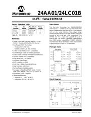
MICROCHIP 24LC01B/SN EEPROM, AEC-Q100, 1 Kbit, 128 x 8位, 400 kHz, I2C, SOIC, 8 引脚
Pictures:
3D模型
符号图
焊盘图
引脚图
产品图
页面导航:
引脚图在P5Hot
标记信息在P13P14
封装信息在P13P31
功能描述在P6
导航目录
24LC01B/SN数据手册
Page:
of 34 Go
若手册格式错乱,请下载阅览PDF原文件
2009 Microchip Technology Inc. DS21711J-page 3
24AA01/24LC01B
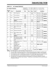
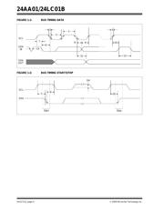
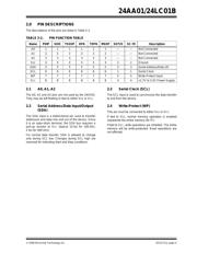
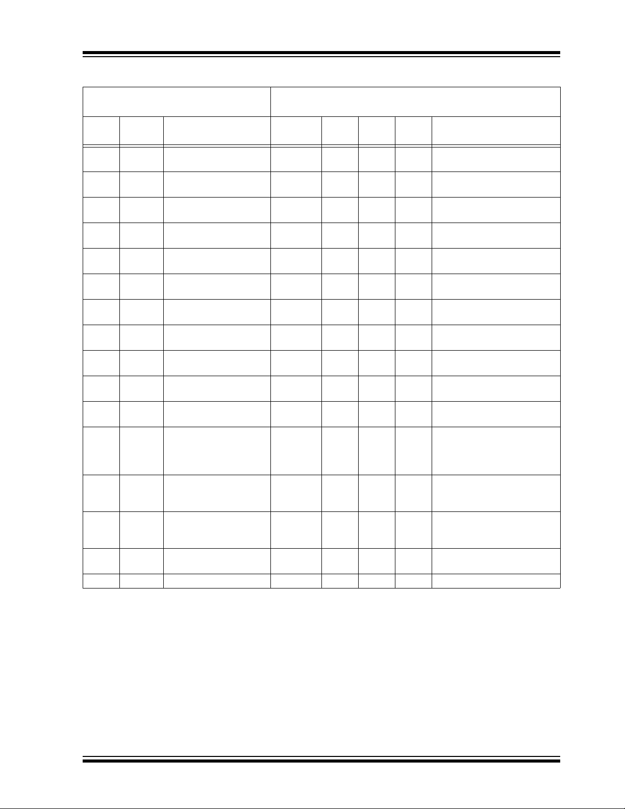
TABLE 1-2: AC CHARACTERISTICS
AC CHARACTERISTICS
Industrial (I): T
A = -40°C to +85°C, VCC = +1.7V to +5.5V
Automotive (E): T
A = -40°C to +125°C, VCC = +2.5V to +5.5V
Param.
No.
Sym. Characteristic Min. Typ. Max. Units Conditions
1F
CLK Clock frequency —
—
—
—
400
100
kHz 2.5V VCC 5.5V
1.7V V
CC 2.5V (24AA01)
2T
HIGH Clock high time 600
4000
—
—
—
—
ns 2.5V VCC 5.5V
1.7V V
CC 2.5V (24AA01)
3TLOW Clock low time 1300
4700
—
—
—
—
ns 2.5V VCC 5.5V
1.7V V
CC 2.5V (24AA01)
4TR SDA and SCL rise time
(Note 1)
—
—
—
—
300
1000
ns 2.5V VCC 5.5V
1.7V V
CC 2.5V (24AA01)
5T
F SDA and SCL fall time — —
—
300 ns (Note 1)
6T
HD:STA Start condition hold time 600
4000
—
—
—
—
ns 2.5V VCC 5.5V
1.7V V
CC 2.5V (24AA01)
7TSU:STA Start condition setup
time
600
4700
—
—
—
—
ns 2.5V VCC 5.5V
1.7V V
CC 2.5V (24AA01)
8T
HD:DAT Data input hold time 0 —
—
—ns(Note 2)
9T
SU:DAT Data input setup time 100
250
—
—
—
—
ns 2.5V VCC 5.5V
1.7V V
CC 2.5V (24AA01)
10 TSU:STO Stop condition setup
time
600
4000
—
—
—
—
ns 2.5V VCC 5.5V
1.7V V
CC 2.5V (24AA01)
11 T
AA Output valid from clock
(Note 2)
—
—
—
—
900
3500
ns 2.5V VCC 5.5V
1.7V V
CC 2.5V (24AA01)
12 TBUF Bus free-time: Time the
bus must be free before
a new transmission can
start
1300
4700
—
—
—
—
ns 2.5V VCC 5.5V
1.7V V
CC 2.5V (24AA01)
13 TOF Output fall time from VIH
minimum to V
IL
maximum
20+0.1C
B
—
—
—
250
250
ns 2.5V V
CC 5.5V
1.7V V
CC 2.5V (24AA01)
14 T
SP Input filter spike
suppression
(SDA and SCL pins)
— — 50 ns (Notes 1 and 3)
15 T
WC Write cycle time
(byte or page)
——5ms—
16 — Endurance 1M — — cycles 25°C, (Note 4)
Note 1: Not 100% tested. C
B = total capacitance of one bus line in pF.
2: As a transmitter, the device must provide an internal minimum delay time to bridge the undefined region
(minimum 300 ns) of the falling edge of SCL to avoid unintended generation of Start or Stop conditions.
3: The combined T
SP and VHYS specifications are due to new Schmitt Trigger inputs which provide improved
noise spike suppression. This eliminates the need for a
TI specification for standard operation.
4: This parameter is not tested but ensured by characterization. For endurance estimates in a specific
application, please consult the Total Endurance™ Model which can be obtained from Microchip’s web site
at www.microchip.com.
器件 Datasheet 文档搜索
AiEMA 数据库涵盖高达 72,405,303 个元件的数据手册,每天更新 5,000 多个 PDF 文件
