Datasheet 搜索 > EEPROM芯片 > Microchip(微芯) > 24LC01B/SN 数据手册 > 24LC01B/SN 数据手册 6/34 页
 器件3D模型
¥ 2.196
24LC01B/SN 数据手册 - Microchip(微芯)
制造商:
Microchip(微芯)
分类:
EEPROM芯片
封装:
SOIC-8
描述:
MICROCHIP 24LC01B/SN EEPROM, AEC-Q100, 1 Kbit, 128 x 8位, 400 kHz, I2C, SOIC, 8 引脚
Pictures:
3D模型
符号图
焊盘图
引脚图
产品图
页面导航:
引脚图在P5Hot
标记信息在P13P14
封装信息在P13P31
功能描述在P6

导航目录
24LC01B/SN数据手册
Page:
of 34 Go
若手册格式错乱,请下载阅览PDF原文件
24AA01/24LC01B
DS21711J-page 6 2009 Microchip Technology Inc.
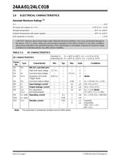
3.0 FUNCTIONAL DESCRIPTION
The 24XX01 supports a bidirectional, 2-wire bus and
data transmission protocol. A device that sends data
onto the bus is defined as transmitter, while defining a
device receiving data as a receiver. The bus has to be
controlled by a master device which generates the
Serial Clock (SCL), controls the bus access and
generates the Start and Stop conditions, while the
24XX01 works as slave. Both master and slave can
operate as transmitter or receiver, but the master
device determines which mode is activated.
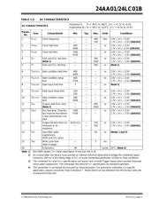
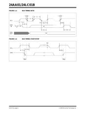
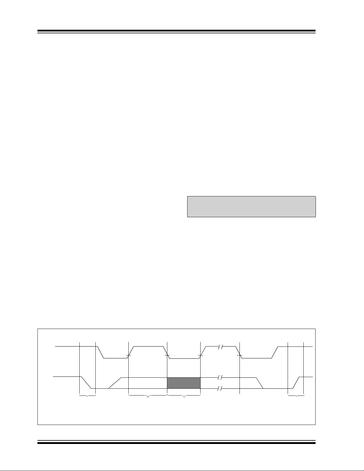
4.0 BUS CHARACTERISTICS
The following bus protocol has been defined:
• Data transfer may be initiated only when the bus
is not busy.
• During data transfer, the data line must remain
stable whenever the clock line is high. Changes in
the data line while the clock line is high will be
interpreted as a Start or Stop condition.
Accordingly, the following bus conditions have been
defined (Figure 4-1).
4.1 Bus Not Busy (A)
Both data and clock lines remain high.
4.2 Start Data Transfer (B)
A high-to-low transition of the SDA line while the clock
(SCL) is high determines a Start condition. All
commands must be preceded by a Start condition.
4.3 Stop Data Transfer (C)
A low-to-high transition of the SDA line while the clock
(SCL) is high determines a Stop condition. All
operations must be ended with a Stop condition.
4.4 Data Valid (D)
The state of the data line represents valid data when,
after a Start condition, the data line is stable for the
duration of the high period of the clock signal.
The data on the line must be changed during the low
period of the clock signal. There is one clock pulse per
bit of data.
Each data transfer is initiated with a Start condition and
terminated with a Stop condition. The number of data
bytes transferred between the Start and Stop
conditions is determined by the master device and is,
theoretically, unlimited (although only the last sixteen
will be stored when doing a write operation). When an
overwrite does occur, it will replace data in a first-in
first-out (FIFO) fashion.
4.5 Acknowledge
Each receiving device, when addressed, is obliged to
generate an acknowledge after the reception of each
byte. The master device must generate an extra clock
pulse which is associated with this Acknowledge bit.
The device that acknowledges has to pull down the
SDA line during the acknowledge clock pulse in such a
way that the SDA line is stable-low during the high
period of the acknowledge-related clock pulse. Of
course, setup and hold times must be taken into
account. During reads, a master must signal an end of
data to the slave by not generating an Acknowledge bit
on the last byte that has been clocked out of the slave.
In this case, the slave (24XX01) will leave the data line
high to enable the master to generate the Stop
condition.
FIGURE 4-1: DATA TRANSFER SEQUENCE ON THE SERIAL BUS
Note: The 24XX01 does not generate any
Acknowledge bits if an internal
programming cycle is in progress.
SCL
SDA
(A) (B) (D) (D) (A)(C)
Start
Condition
Address or
Acknowledge
Valid
Data
Allowed
to Change
Stop
Condition
器件 Datasheet 文档搜索
AiEMA 数据库涵盖高达 72,405,303 个元件的数据手册,每天更新 5,000 多个 PDF 文件
