Datasheet 搜索 > CPLD芯片 > Altera(阿尔特拉) > 5M160ZE64C5N 数据手册 > 5M160ZE64C5N 数据手册 130/167 页

¥ 19.984
5M160ZE64C5N 数据手册 - Altera(阿尔特拉)
制造商:
Altera(阿尔特拉)
分类:
CPLD芯片
封装:
QFP-64
描述:
ALTERA 5M160ZE64C5N 可编程逻辑芯片, CPLD, MAX V系列, 160 LE, 64EQFP
Pictures:
3D模型
符号图
焊盘图
引脚图
产品图
页面导航:
引脚图在P118P128P140P150Hot
典型应用电路图在P13P20P21P22P23P24P25P128
原理图在P14
型号编码规则在P9
功能描述在P13P14P15P105P107P108P109P110P111
技术参数、封装参数在P44P49P51P53P54P55P56P58P59P60P61P62
电气规格在P44P49P51P52
型号编号列表在P49
导航目录
5M160ZE64C5N数据手册
Page:
of 167 Go
若手册格式错乱,请下载阅览PDF原文件
7–26 Chapter 7: User Flash Memory in MAX V Devices
Software Support for UFM Block
MAX V Device Handbook January 2011 Altera Corporation
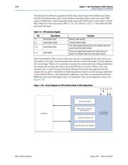
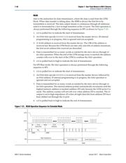
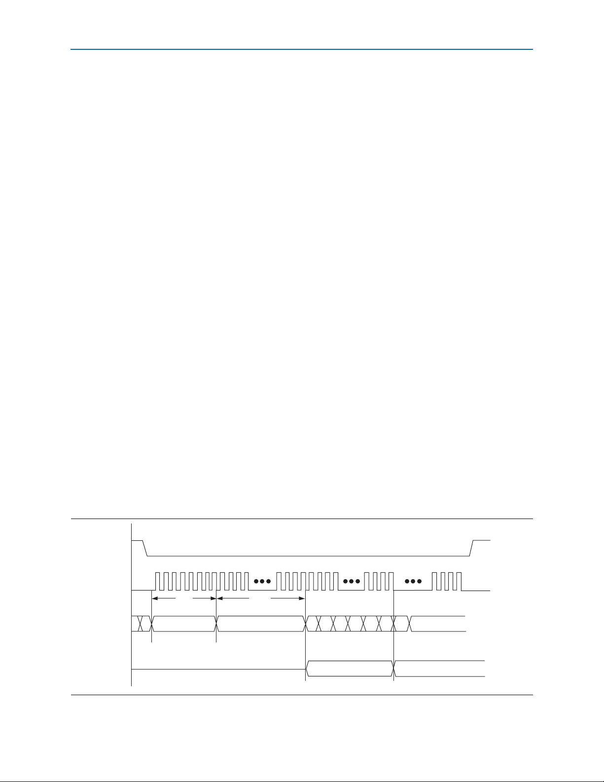
READ
READ
is the instruction for data transmission, where the data is read from the UFM
block. When data transfer is taking place, the MSB is always the first bit to be
transmitted or received. The data output stream is continuous through all addresses
until it is terminated by a low-to-high transition at the
nCS
port. The
READ
operation is
always performed through the following sequence in SPI, as shown in Figure 7–21:
1.
nCS
is pulled low to indicate the start of transmission.
2. An 8-bit
READ
opcode (
00000011
) is received from the master device. (If internal
programming is in progress,
READ
is ignored and not accepted).
3. A 16-bit address is received from the master device. The LSB of the address is
received last. Because the UFM block can take only nine bits of address maximum,
the first seven address bits received are discarded.
4. Data is transmitted for as many words as needed by the slave device through
SO
for
READ
operation. When the end of the UFM storage array is reached, the address
counter rolls over to the start of the UFM to continue the
READ
operation.
5.
nCS
is pulled back to high to indicate the end of transmission.
For SPI Base mode, the
READ
operation is always performed through the following
sequence in SPI:
1.
nCS
is pulled low to indicate the start of transmission.
2. An 8-bit
READ
opcode (
00000011
) is received from the master device, followed by
an 8-bit address. If internal programming is in progress, the
READ
operation is
ignored and not accepted.
3. Data is transmitted for as many words as needed by the slave device through
SO
for
READ
operation. The internal address pointer automatically increments until the
highest memory address is reached (address 255 only because the UFM sector 0 is
used). The address counter will not roll over when address 255 is reached. The
SO
output is set to high-impedance (Z) when all eight data bits from address 255 have
been shifted out through the
SO
port.
4.
nCS
is pulled back to high to indicate the end of transmission.
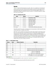
Figure 7–21. READ Operation Sequence for Extended Mode
0123 45678 9
10 11 20 21 22 23 24 25 26 27 36 37 38 39
nCS
SCK
SI
SO
High Impedance
03
H
MSB
MSB MSB
MSB
16-bit Data Out 1 16-bit Data Out 2
8-bit
Instruction
16-bit
Address
器件 Datasheet 文档搜索
AiEMA 数据库涵盖高达 72,405,303 个元件的数据手册,每天更新 5,000 多个 PDF 文件
