Datasheet 搜索 > 逻辑控制器 > Nexperia(安世) > 74AHCT595PW,112 数据手册 > 74AHCT595PW,112 数据手册 5/23 页
 器件3D模型
¥ 0.312
74AHCT595PW,112 数据手册 - Nexperia(安世)
制造商:
Nexperia(安世)
分类:
逻辑控制器
封装:
TSSOP-16
Pictures:
3D模型
符号图
焊盘图
引脚图
产品图
页面导航:
导航目录
74AHCT595PW,112数据手册
Page:
of 23 Go
若手册格式错乱,请下载阅览PDF原文件
74AHC_AHCT595 All information provided in this document is subject to legal disclaimers. © NXP B.V. 2012. All rights reserved.
Product data sheet Rev. 5 — 4 July 2012 4 of 22
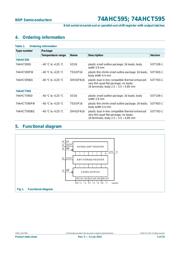
NXP Semiconductors
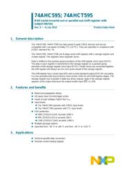
74AHC595; 74AHCT595
8-bit serial-in/serial-out or parallel-out shift register with output latches
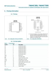
6. Pinning information
6.1 Pinning
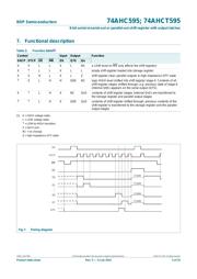
6.2 Pin description
(1) This is not a supply pin. The substrate is attached to this
pad using conductive die attach material. There is no
electrical or mechanical requirement to solder this pad.
However, if it is soldered, the solder land should remain
floating or be connected to GND.
Fig 5. Pin configuration SO16 and TSSOP16 Fig 6. Pin configuration DHVQFN16
74AHC595
74AHCT595
Q1 V
CC
Q2 Q0
Q3 DS
Q4 OE
Q5 STCP
Q6 SHCP
Q7 MR
GND Q7S
001aae538
1
2
3
4
5
6
7
8
10
9
12
11
14
13
16
15
001aae483
74AHC595
74AHCT595
Q7 MR
Q6 SHCP
Q5 STCP
Q4 OE
Q3 DS
Q2 Q0
GND
Q7S
Q1
V
CC
Transparent top view
7 10
6 11
5 12
4
13
3 14
2 15
8
9
1
16
terminal 1
index area
GND
(1)
Table 2. Pin description
Symbol Pin Description
Q1 1 parallel data output 1
Q2 2 parallel data output 2
Q3 3 parallel data output 3
Q4 4 parallel data output 4
Q5 5 parallel data output 5
Q6 6 parallel data output 6
Q7 7 parallel data output 7
GND 8 ground (0 V)
Q7S 9 serial data output
MR
10 master reset (active LOW)
SHCP 11 shift register clock input
STCP 12 storage register clock input
OE
13 output enable input (active LOW)
DS 14 serial data input
Q0 15 parallel data output 0
V
CC
16 supply voltage
器件 Datasheet 文档搜索
AiEMA 数据库涵盖高达 72,405,303 个元件的数据手册,每天更新 5,000 多个 PDF 文件
