Datasheet 搜索 > 移位寄存器 > NXP(恩智浦) > 74AHCT595PW,118 数据手册 > 74AHCT595PW,118 数据手册 5/25 页

 器件3D模型
¥ 0.806
74AHCT595PW,118 数据手册 - NXP(恩智浦)
制造商:
NXP(恩智浦)
分类:
移位寄存器
封装:
TSSOP-16
描述:
NXP 74AHCT595PW,118 移位寄存器, AHCT系列, 高速CMOS, 串行至并行、串行至串行, 1元件, TSSOP, 16 引脚, 4.5 V, 5.5 V
Pictures:
3D模型
符号图
焊盘图
引脚图
产品图
页面导航:
引脚图在P3Hot
典型应用电路图在P11P12
原理图在P1P9P11
封装尺寸在P14P16P17
标记信息在P14P15
封装信息在P13P14P15P16P17
技术参数、封装参数在P4
应用领域在P1P25
电气规格在P5


导航目录
74AHCT595PW,118数据手册
Page:
of 25 Go
若手册格式错乱,请下载阅览PDF原文件
SN54AHCT595
,
SN74AHCT595
www.ti.com
SCLS374N –MAY 1997–REVISED JULY 2014
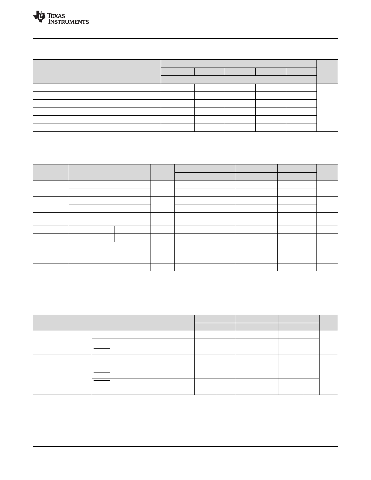
7.4 Thermal Information
SN74AHCT595
THERMAL METRIC
(1)
D DB N NS PW UNIT
16 PINS
R
θJA
Junction-to-ambient thermal resistance 80.2 97.5 47.5 79.1 105.7
R
θJC(top)
Junction-to-case (top) thermal resistance 39.1 47.7 34.9 35.4 40.4
R
θJB
Junction-to-board thermal resistance 27.7 48.1 27.5 39.9 50.7
°C/W
ψ
JT
Junction-to-top characterization parameter 9.9 9.8 19.8 5.4 3.7
ψ
JB
Junction-to-board characterization parameter 37.4 47.6 27.4 39.5 50.1
R
θJC(bot)
Junction-to-case (bottom) thermal resistance n/a n/a n/a n/a n/a
(1) For more information about traditional and new thermal metrics, see the IC Package Thermal Metrics application report, SPRA953.
7.5 Electrical Characteristics
over operating free-air temperature range (unless otherwise noted)
T
A
= 25°C SN54AHCT595
(1)
SN74AHCT595
PARAMETER TEST CONDITIONS V
CC
UNIT
MIN TYP MAX MIN MAX MIN MAX
I
OH
= –50 mA 4.4 4.5 4.4 4.4
V
OH
4.5 V V
I
OH
= –8 mA 3.94 3.8 3.8
I
OL
= 50 µA 0.1 0.1 0.1
V
OL
4.5 V V
I
OL
= 8 mA 0.36 0.44 0.44
0 to 5.5
I
I
V
I
= 5.5 V or GND ±0.1 ±1
(2)
±1 µA
V
I
OZ
V
O
= V
CC
or GND Q
A
– Q
H
5.5 V ±0.25 ±2.5 ±2.5 µA
I
CC
V
I
= V
CC
or GND I
O
= 0 5.5 V 4 40 40 µA
One input at 3.4V,
ΔI
CC
(3)
5.5 V 2 2.2 2.2 mA
Other inputs at V
CC
or GND
C
i
V
I
= V
CC
or GND 5 V 3 10 10 pF
C
o
V
O
= V
CC
or GND 5 V 5.5 pF
(1) Product Preview
(2) On products compliant to MIL-PRF-38535, this parameter is not production tested at V
CC
= 0 V.
(3) This is the increase in supply current for each input at one of the specified TTL voltage levels, rather than 0 V or V
CC
.
7.6 Timing Requirements
over recommended operating free-air temperature range, V
CC
= 5 V ± 0.5 V (unless otherwise noted) (see Figure 3)
T
A
= 25°C SN54AHCT595
(1)
SN74AHCT595
PARAMETER UNIT
MIN MAX MIN MAX MIN MAX
SRCLK high or low 5 5.5 5.5
t
w
Pulse duration RCLK high or low 5 5.5 5.5 ns
SRCLR low 5 5 5
SER before SRCLK↑ 3 3 3
SRCLK↑ before RCLK↑
(2)
5 5 5
t
su
Setup time ns
SRCLR low before RCLK↑ 5 5 5
SRCLR high (inactive) before SRCLK↑ 3.4 3.8 3.8
t
h
Hold time SER after SRCLK↑ 2 2 2 ns
(1) Product Preview
(2) This setup time allows the storage register to receive stable data from the shift register. The clocks can be tied together, in which case
the shift register is one clock pulse ahead of the storage register.
Copyright © 1997–2014, Texas Instruments Incorporated Submit Documentation Feedback 5
Product Folder Links: SN54AHCT595 SN74AHCT595
器件 Datasheet 文档搜索
AiEMA 数据库涵盖高达 72,405,303 个元件的数据手册,每天更新 5,000 多个 PDF 文件
