Datasheet 搜索 > 逻辑控制器 > TI(德州仪器) > 74AVC8T245RHLRG4 数据手册 > 74AVC8T245RHLRG4 数据手册 1/29 页

¥ 2.702
74AVC8T245RHLRG4 数据手册 - TI(德州仪器)
制造商:
TI(德州仪器)
分类:
逻辑控制器
封装:
VQFN-24
描述:
可配置电压转换和3态输出的8位双电源总线收发器 8-BIT DUAL-SUPPLY BUS TRANSCEIVER WITH CONFIGURABLE VOLTAGE TRANSLATION AND 3-STATE OUTPUTS
Pictures:
3D模型
符号图
焊盘图
引脚图
产品图
页面导航:
引脚图在P3Hot
典型应用电路图在P1P14P15
原理图在P13P14
封装尺寸在P19P21P22
标记信息在P19P20
封装信息在P18P19P20P21P22
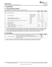
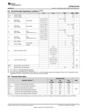
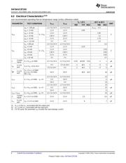
技术参数、封装参数在P4
应用领域在P1P29
电气规格在P6
导航目录
74AVC8T245RHLRG4数据手册
Page:
of 29 Go
若手册格式错乱,请下载阅览PDF原文件
DIR
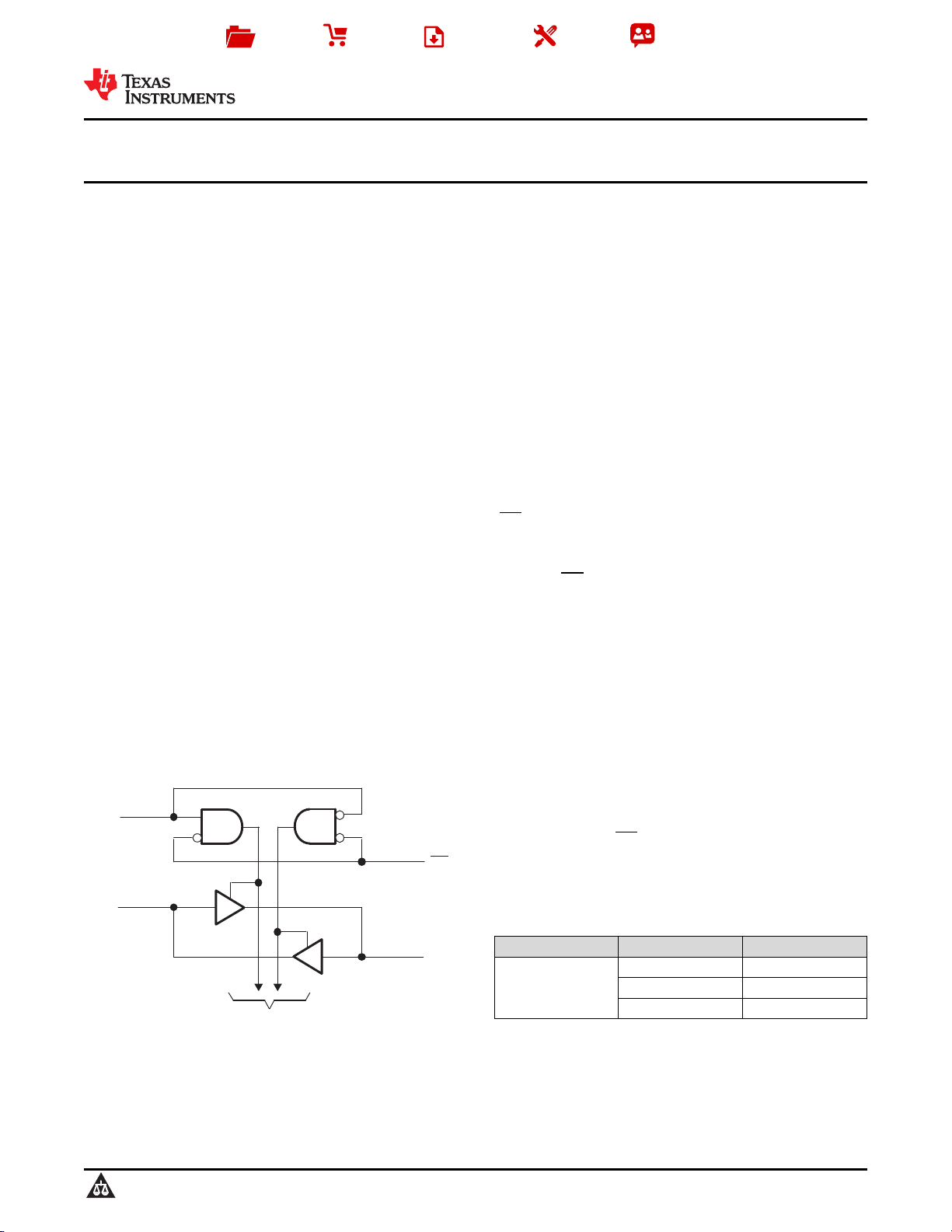
OE
A1
B1
To Seven Other Channels
2
3
22
21
Product
Folder
Sample &
Buy
Technical
Documents
Tools &
Software
Support &
Community
SN74AVC8T245
SCES517I –DECEMBER 2003–REVISED DECEMBER 2014
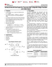
SN74AVC8T245 8-Bit Dual-Supply Bus Transceiver With Configurable Voltage Translation
and 3-State Outputs
1 Features 3 Description
This 8-bit noninverting bus transceiver uses two
1
• Control Inputs V
IH
/V
IL
Levels Are Referenced to
separate configurable power-supply rails. The
V
CCA
Voltage
SN74AVC8T245 is optimized to operate with
• V
CC
Isolation Feature – If Either V
CC
Input Is at
V
CCA
/V
CCB
set at 1.4 V to 3.6 V. The device is
GND, All I/O Ports Are in the High-Impedance
operational with V
CCA
/V
CCB
as low as 1.2 V. The A
State
port is designed to track V
CCA
. V
CCA
accepts any
supply voltage from 1.2 V to 3.6 V. The B port is
• I
off
Supports Partial Power-Down Mode Operation
designed to track V
CCB
. V
CCB
accepts any supply
• Fully Configurable Dual-Rail Design Allows Each
voltage from 1.2 V to 3.6 V. This allows for universal
Port to Operate Over the Full 1.4-V to 3.6-V
low-voltage bidirectional translation between any of
Power-Supply Range
the 1.2-V, 1.5-V, 1.8-V, 2.5-V, and 3.3-V voltage
• I/Os Are 4.6-V Tolerant
nodes.
• Maximum Data Rates
The SN74AVC8T245 is designed for asynchronous
– 170 Mbps (V
CCA
< 1.8 V or V
CCB
< 1.8 V)
communication between data buses. The device
transmits data from the A bus to the B bus or from
– 320 Mbps (V
CCA
≥ 1.8 V and V
CCB
≥ 1.8 V)
the B bus to the A bus, depending on the logic level
• Latch-Up Performance Exceeds 100 mA Per
at the direction-control (DIR) input. The output-enable
JESD 78, Class II
(OE) input can be used to disable the outputs so the
• ESD Protection Exceeds JESD 22
buses are effectively isolated.
– 8000-V Human-Body Model (A114-A)
The SN74AVC8T245 is designed so the control pins
(DIR and OE) are supplied by V
CCA
.
– 200-V Machine Model (A115-A)
– 1000-V Charged-Device Model (C101)
The SN74AVC8T245 solution is compatible with a
single-supply system and can be replaced later with a
2 Applications
'245 function, with minimal printed circuit board
redesign.
• Personal Electronic
This device is fully specified for partial-power-down
• Industrial
applications using I
off
. The I
off
circuitry disables the
• Enterprise
outputs, thus preventing damaging current backflow
• Telecom
through the device when it is powered down.
The V
CC
isolation feature ensures that if either V
CC
Logic Diagram (Positive Logic)
input is at GND, both ports are in the high-impedance
state.
To ensure the high-impedance state during power up
or power down, OE shall be tied to V
CC
through a
pullup resistor; the minimum value of the resistor is
determined by the current-sinking capability of the
driver.
Device Information
(1)
PART NUMBER PACKAGE BODY SIZE (NOM)
VQFN (24) 3.50 mm x 5.50 mm
SN74AVC8T245 TSSOP (24) 4.40 mm x 7.80 mm
TVSOP (24) 4.40 mm x 5.00 mm
(1) For all available packages, see the orderable addendum at
the end of the datasheet.
1
An IMPORTANT NOTICE at the end of this data sheet addresses availability, warranty, changes, use in safety-critical applications,
intellectual property matters and other important disclaimers. PRODUCTION DATA.
器件 Datasheet 文档搜索
AiEMA 数据库涵盖高达 72,405,303 个元件的数据手册,每天更新 5,000 多个 PDF 文件
