Datasheet 搜索 > FPGA芯片 > Microsemi(美高森美) > A42MX16-3TQG176 数据手册 > A42MX16-3TQG176 数据手册 88/150 页
 器件3D模型
¥ 952.999
A42MX16-3TQG176 数据手册 - Microsemi(美高森美)
制造商:
Microsemi(美高森美)
分类:
FPGA芯片
封装:
TQFP-176
Pictures:
3D模型
符号图
焊盘图
引脚图
产品图
页面导航:
引脚图在P18P20P88P90P91P92P94P96P98P100P102P104Hot
型号编码规则在P2P146
封装信息在P2P148
功能描述在P1P6P147
技术参数、封装参数在P22P23P24P25P26P27P28P29P146P148
电气规格在P23P25P27P146P148
导航目录
A42MX16-3TQG176数据手册
Page:
of 150 Go
若手册格式错乱,请下载阅览PDF原文件
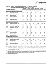
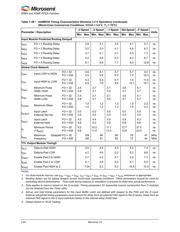
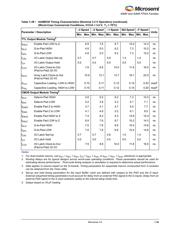
40MX and 42MX FPGA Families
1-83 Revision 13
Pin Descriptions
CLK/A/B, I/O Global Clock
Clock inputs for clock distribution networks. CLK is for 40MX while CLKA and CLKB are for 42MX devices. The clock
input is buffered prior to clocking the logic modules. This pin can also be used as an I/O.
DCLK, I/O Diagnostic Clock
Clock input for diagnostic probe and device programming. DCLK is active when the MODE pin is HIGH. This pin
functions as an I/O when the MODE pin is LOW.
GND Ground
Input LOW supply voltage.
I/O Input/Output
Input, output, tristate or bidirectional buffer. Input and output levels are compatible with standard TTL and CMOS
specifications. Unused I/Os pins are configured by the Designer software as shown in Table 1-40.
In all cases, it is recommended to tie all unused MX I/O pins to LOW on the board. This applies to all dual-purpose pins
when configured as I/Os as well.
LP Low Power Mode
Controls the low power mode of all 42MX devices. The device is placed in the low power mode by connecting the LP
pin to logic HIGH. In low power mode, all I/Os are tristated, all input buffers are turned OFF, and the core of the device
is turned OFF. To exit the low power mode, the LP pin must be set LOW. The device enters the low power mode 800 ns
after the LP pin is driven to a logic HIGH. It will resume normal operation in 200 µs after the LP pin is driven to a logic
LOW.
MODE Mode
Controls the use of multifunction pins (DCLK, PRA, PRB, SDI, TDO). The MODE pin is held HIGH to provide
verification capability. The MODE pin should be terminated to GND through a 10k resistor so that the MODE pin can
be pulled HIGH when required.
NC No Connection
This pin is not connected to circuitry within the device. These pins can be driven to any voltage or can be left floating
with no effect on the operation of the device.
PRA, I/O
PRB, I/O Probe A/B
The Probe pin is used to output data from any user-defined design node within the device. Each diagnostic pin can be
used in conjunction with the other probe pin to allow real-time diagnostic output of any signal path within the device.
The Probe pin can be used as a user-defined I/O when verification has been completed. The pin's probe capabilities
can be permanently disabled to protect programmed design confidentiality. The Probe pin is accessible when the
MODE pin is HIGH. This pin functions as an I/O when the MODE pin is LOW.
QCLKA/B/C/D, I/O Quadrant Clock
Quadrant clock inputs for A42MX36 devices. When not used as a register control signal, these pins can function as
user I/Os.
Table 1-40 • Configuration of Unused I/Os
Device Configuration
A40MX02, A40MX04 Pulled LOW
A42MX09, A42MX16 Pulled LOW
A42MX24, A42MX36 Tristated
器件 Datasheet 文档搜索
AiEMA 数据库涵盖高达 72,405,303 个元件的数据手册,每天更新 5,000 多个 PDF 文件
