Datasheet 搜索 > FPGA芯片 > Microsemi(美高森美) > A42MX16-3VQ100 数据手册 > A42MX16-3VQ100 数据手册 6/150 页
 器件3D模型
¥ 1029.059
A42MX16-3VQ100 数据手册 - Microsemi(美高森美)
制造商:
Microsemi(美高森美)
分类:
FPGA芯片
封装:
TQFP-100
Pictures:
3D模型
符号图
焊盘图
引脚图
产品图
页面导航:
引脚图在P18P20P88P90P91P92P94P96P98P100P102P104Hot
型号编码规则在P2P146
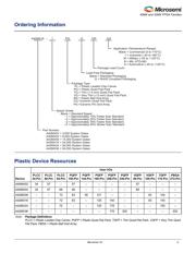
封装信息在P2P148
功能描述在P1P6P147
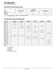
技术参数、封装参数在P22P23P24P25P26P27P28P29P146P148
电气规格在P23P25P27P146P148
导航目录
A42MX16-3VQ100数据手册
Page:
of 150 Go
若手册格式错乱,请下载阅览PDF原文件

Revision 13 1-1
1 – 40MX and 42MX FPGA Families
General Description
Microsemi's 40MX and 42MX families offer a cost-effective design solution at 5V. The MX devices are single-chip
solutions and provide high performance while shortening the system design and development cycle. MX devices can
integrate and consolidate logic implemented in multiple PALs, CPLDs, and FPGAs. Example applications include high-
speed controllers and address decoding, peripheral bus interfaces, DSP, and co-processor functions.
The MX device architecture is based on Microsemi’s patented antifuse technology implemented in a 0.45µm triple-
metal CMOS process. With capacities ranging from 3,000 to 54,000 system gates, the MX devices provide
performance up to 250 MHz, are live on power-up and have one-fifth the standby power consumption of comparable
FPGAs. MX FPGAs provide up to 202 user I/Os and are available in a wide variety of packages and speed grades.
A42MX24 and A42MX36 devices also feature MultiPlex I/Os, which support mixed-voltage systems, enable
programmable PCI, deliver high-performance operation at both 5.0V and 3.3V, and provide a low-power mode. The
devices are fully compliant with the PCI Local Bus Specification (version 2.1). They deliver 200 MHz on-chip operation
and 6.1 ns clock-to-output performance.
The 42MX24 and 42MX36 devices include system-level features such as IEEE Standard 1149.1 (JTAG) Boundary
Scan Testing and fast wide-decode modules. In addition, the A42MX36 device offers dual-port SRAM for implementing
fast FIFOs, LIFOs, and temporary data storage. The storage elements can efficiently address applications requiring
wide datapath manipulation and can perform transformation functions such as those required for telecommunications,
networking, and DSP.
All MX devices are fully tested over automotive and military temperature ranges. In addition, the largest member of the
family, the A42MX36, is available in both CQ208 and CQ256 ceramic packages screened to MIL-STD-883 levels. For
easy prototyping and conversion from plastic to ceramic, the CQ208 and PQ208 devices are pin-compatible.
MX Architectural Overview
The MX devices are composed of fine-grained building blocks that enable fast, efficient logic designs. All devices
within these families are composed of logic modules, I/O modules, routing resources and clock networks, which are
the building blocks for fast logic designs. In addition, the A42MX36 device contains embedded dual-port SRAM
modules, which are optimized for high-speed datapath functions such as FIFOs, LIFOs and scratchpad memory.
A42MX24 and A42MX36 also contain wide-decode modules.
Logic Modules
The 40MX logic module is an eight-input, one-output logic circuit designed to implement a wide range of logic functions
with efficient use of interconnect routing resources (Figure 1-1 on page 1-2).
The logic module can implement the four basic logic functions (NAND, AND, OR and NOR) in gates of two, three, or
four inputs. The logic module can also implement a variety of D-latches, exclusivity functions, AND-ORs and OR-
ANDs. No dedicated hard-wired latches or flip-flops are required in the array; latches and flip-flops can be constructed
from logic modules whenever required in the application.
器件 Datasheet 文档搜索
AiEMA 数据库涵盖高达 72,405,303 个元件的数据手册,每天更新 5,000 多个 PDF 文件
