Datasheet 搜索 > 放大器、缓冲器 > ADI(亚德诺) > AD210AN 数据手册 > AD210AN 数据手册 4/8 页
 器件3D模型
¥ 1622.058
AD210AN 数据手册 - ADI(亚德诺)
制造商:
ADI(亚德诺)
分类:
放大器、缓冲器
封装:
PDIP-12
描述:
Analog Devices### 隔离放大器
Pictures:
3D模型
符号图
焊盘图
引脚图
产品图
页面导航:
导航目录
AD210AN数据手册
Page:
of 8 Go
若手册格式错乱,请下载阅览PDF原文件
AD210
REV. A
–4–
low side of the signal source. This will not work if the source has
another current path to input common or if current flows in the
signal source LO lead. To minimize CMR degradation, keep the
resistor in series with the input LO below a few hundred ohms.
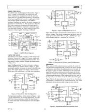
Figure 5 also shows the preferred gain adjustment circuit. The
circuit shows R
F
of 50 kΩ, and will work for gains of ten or
greater. The adjustment becomes less effective at lower gains
(its effect is halved at G = 2) so that the pot will have to be a
larger fraction of the total R
F
at low gain. At G = 1 (follower)
the gain cannot be adjusted downward without compromising
input impedance; it is better to adjust gain at the signal source
or after the output.
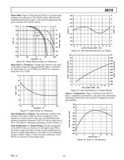
Figure 6 shows the input adjustment circuit for use when the
input amplifier is configured in the inverting mode. The offset
adjustment nulls the voltage at the summing node. This is pref-
erable to current injection because it is less affected by subse-
quent gain adjustment. Gain adjustment is made in the feedback
and will work for gains from 1 V/V to 100 V/V.
19
15
16
17
18
30
29
+V
OSS
AD210
+V
ISS
–V
ISS
+15V
2
3
4
–V
OSS
V
OUT
V
SIG
14
200Ω
47.5kΩ
5kΩ
100kΩ
GAIN
OFFSET
50kΩ
R
S
1
Figure 6. Adjustments for Inverting Input
Figure 7 shows how offset adjustments can be made at the out-
put, by offsetting the floating output port. In this circuit, ±15 V
would be supplied by a separate source. The AD210’s output
amplifier is fixed at unity, therefore, output gain must be made
in a subsequent stage.
19
15
16
17
18
30
29
+V
OSS
AD210
+V
ISS
–V
ISS
+15V
2
3
4
–V
OSS
V
OUT
14
200Ω
1
0.1µF
100k
OFFSET
50kΩ
+15V
–15V
Figure 7. Output-Side Offset Adjustment
PCB Layout for Multichannel Applications: The unique
pinout positioning minimizes board space constraints for multi-
channel applications. Figure 8 shows the recommended printed
circuit board layout for a noninverting input configuration with
gain.
R
F
R
G
R
F
R
G
R
F
R
G
POWER
CHANNEL INPUTS
1
2
3
0.1"
GRID
CHANNEL OUTPUTS
1
2
3
Figure 8. PCB Layout for Multichannel Applications with
Gain
Synchronization: The AD210 is insensitive to the clock of an
adjacent unit, eliminating the need to synchronize the clocks.
However, in rare instances channel to channel pick-up may
occur if input signal wires are bundled together. If this happens,
shielded input cables are recommended.
PERFORMANCE CHARACTERISTICS
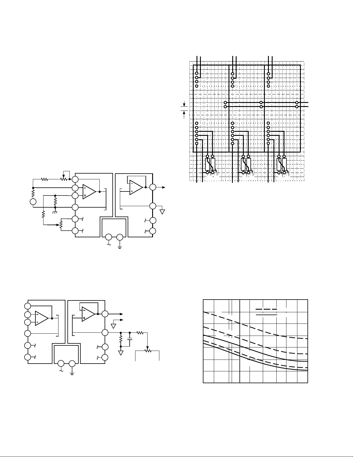
Common-Mode Rejection: Figure 9 shows the common-
mode rejection of the AD210 versus frequency, gain and input
source resistance. For maximum common-mode rejection of
unwanted signals, keep the input source resistance low and care-
fully lay out the input, avoiding excessive stray capacitance at
the input terminals.
180
140
40
10 20 50 60 100 200 500 1k 2k 5k 10k
160
100
120
60
80
FREQUENCY – Hz
R
LO
= 0Ω
R
LO
= 500Ω
R
LO
= 0Ω
R
LO
= 10kΩ
R
LO
= 10kΩ
G = 100
G = 1
CMR – dB
Figure 9. Common-Mode Rejection vs. Frequency
器件 Datasheet 文档搜索
AiEMA 数据库涵盖高达 72,405,303 个元件的数据手册,每天更新 5,000 多个 PDF 文件
