Datasheet 搜索 > 数字电位器 > ADI(亚德诺) > AD5270BRMZ20 数据手册 > AD5270BRMZ20 数据手册 10/24 页

¥ 17.927
AD5270BRMZ20 数据手册 - ADI(亚德诺)
制造商:
ADI(亚德诺)
分类:
数字电位器
封装:
MSOP
Pictures:
3D模型
符号图
焊盘图
引脚图
产品图
页面导航:
引脚图在P10P23Hot
原理图在P1
封装尺寸在P23
型号编码规则在P24
焊接温度在P9
功能描述在P1P10P23
技术参数、封装参数在P1P3P7P9P17P22
应用领域在P1
电气规格在P3P5P11
导航目录
AD5270BRMZ20数据手册
Page:
of 24 Go
若手册格式错乱,请下载阅览PDF原文件
AD5270/AD5271 Data Sheet
Rev. F | Page 10 of 24
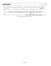
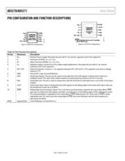
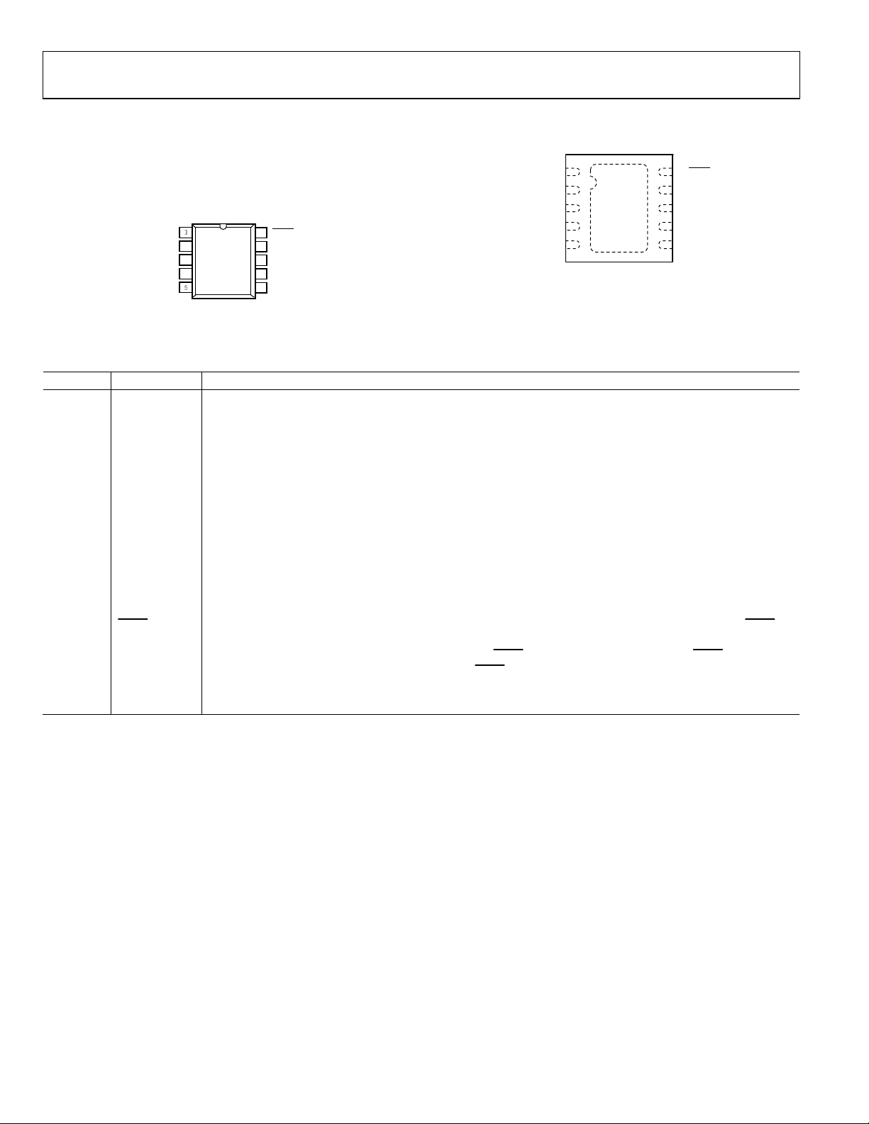
PIN CONFIGURATION AND FUNCTION DESCRIPTIONS
V
DD
1
1
V
SS
2
2
A
3
3
W
4
4
SDO
10
9
8
SCLK
7
5
EXT_CAP
DIN
6
GND
AD5270/
AD5271
TOP VIEW
(Not to Scale)
SYNC
08077-005
Figure 5. MSOP Pin Configuration
SYNC
V
DD
1
V
SS
2
A
3
W
4
SDO
10
9
8
SCLK
7
5
EXT_CAP
DIN
6
GND
NOTES
1.THE EXPOSED PAD IS LEFT FLOATING
OR IS TIED TO V
SS
.
AD5270/
AD5271
(EXPOSED
PAD)
08077-040
Figure 6. LFCSP Pin Configuration
Table 10. Pin Function Descriptions
Pin No. Mnemonic Description
1 V
DD
Positive Power Supply. Decouple this pin with 0.1 μF ceramic capacitors and 10 μF capacitors.
2 A Terminal A of RDAC. V
SS
≤ V
A
≤ V
DD
.
3 W Wiper Terminal of RDAC. V
SS
≤ V
W
≤ V
DD
.
4 V
SS
Negative Supply. Connect to 0 V for single-supply applications. Decouple this pin with 0.1 μF ceramic
capacitors and 10 μF capacitors.
5 EXT_CAP
External Capacitor. Connect a 1 μF capacitor between EXT_CAP and V
SS
. This capacitor must have a voltage
rating of ≥7 V.
6 GND Ground Pin, Logic Ground Reference.
7 SDO
Serial Data Output. This pin can be used to clock data from the shift register in daisy-chain mode or in
readback mode. This open-drain output requires an external pull-up resistor even if it is not use.
8 DIN
Serial Data Line. This pin is used in conjunction with the SCLK line to clock data into or out of the 16-bit input
register.
9 SCLK
Serial Clock Input. Data is clocked into the shift register on the falling edge of the serial clock input. Data can
be transferred at rates up to 50 MHz.
10
SYNC
Falling Edge Synchronization Signal. This is the frame synchronization signal for the input data. When SYNC
goes low, it enables the shift register and data is transferred in on the falling edges of the subsequent clocks.
The selected register is updated on the rising edge of SYNC following the 16
th
clock cycle. If SYNC is taken
high before the 16
th
clock cycle, the rising edge of SYNC acts as an interrupt, and the write sequence is
ignored by the RDAC.
EPAD Exposed Pad Leave floating or connected to V
SS
.
器件 Datasheet 文档搜索
AiEMA 数据库涵盖高达 72,405,303 个元件的数据手册,每天更新 5,000 多个 PDF 文件
