Datasheet 搜索 > DA转换器 > ADI(亚德诺) > AD5331BRU-REEL7 数据手册 > AD5331BRU-REEL7 数据手册 21/28 页


¥ 0
AD5331BRU-REEL7 数据手册 - ADI(亚德诺)
制造商:
ADI(亚德诺)
分类:
DA转换器
封装:
TSSOP
描述:
2.5 V至5.5 V , 115 μA ,并行接口单电压输出8位/ 10位/ 12位DAC 2.5 V to 5.5 V, 115 μA, Parallel Interface Single Voltage-Output 8-/10-/12-Bit DACs
Pictures:
3D模型
符号图
焊盘图
引脚图
产品图
页面导航:
引脚图在P7P8P9P10P23Hot
典型应用电路图在P21
原理图在P1P7P8P9P10
封装尺寸在P24
型号编码规则在P25
焊接温度在P6
功能描述在P1P7P8P9P10
技术参数、封装参数在P1P3P6
应用领域在P1P21
电气规格在P13
导航目录
AD5331BRU-REEL7数据手册
Page:
of 28 Go
若手册格式错乱,请下载阅览PDF原文件
AD5330/AD5331/AD5340/AD5341
Rev. A | Page 21 of 28
APPLICATIONS INFORMATION
TYPICAL APPLICATION CIRCUITS
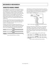
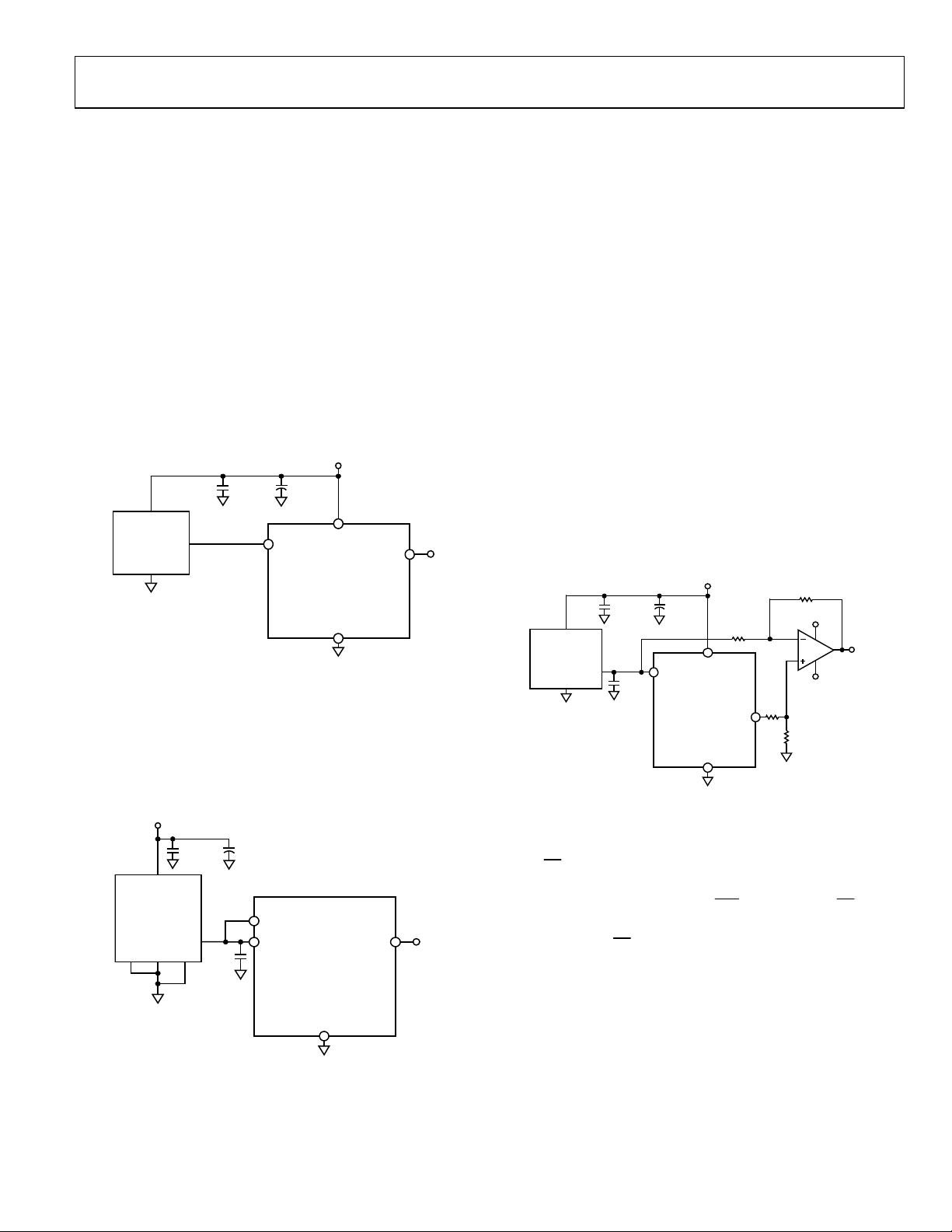
The AD5330/AD5331/AD5340/AD5341 can be used with
a wide range of reference voltages, especially if the reference
inputs are configured to be unbuffered, in which case the
devices offer full, one-quadrant multiplying capability over a
reference range of 0.25 V to V
DD
. More typically, these devices
can be used with a fixed, precision reference voltage. Figure 43
shows a typical setup for the devices when using an external
reference connected to the unbuffered reference inputs. If the
reference inputs are unbuffered, the reference input range is
from 0.25 V to V
DD
, but if the on-chip reference buffers are
used, the reference range is reduced. Suitable references for 5 V
operation are the AD780 and REF192. For 2.5 V operation, a
suitable external reference is the AD589, a 1.23 V band gap
reference.
AD5330/AD5331/
AD5340/AD5341
V
OUT
V
DD
= 2.5V TO 5.5
V
V
DD
GND
V
REF
GND
EXT
REF
+
0.1µF 10µF
V
OUT
V
IN
AD780/REF192
WITH V
DD
= 5V
OR
A
D589 WITH V
DD
= 2.5V
06852-044
Figure 43. AD5330/AD5331/AD5340/AD5341 Using External Reference
DRIVING V
DD
FROM THE REFERENCE VOLTAGE
If an output range of 0 V to V
DD
is required, the simplest
solution is to connect the reference inputs to V
DD
. Because this
supply may not be very accurate and may be noisy, the devices
can be powered from the reference voltage, for example using
a 5 V reference such as the ADP667, as shown in Figure 44.
AD5330/AD5331/
AD5340/AD5341
GND SHDN
V
OUT
ADP667
VSET
6V TO 16
V
V
OUT
V
DD
V
IN
GND
V
REF
+
0.1µF
0.1µF
10µF
06852-045
Figure 44. Using an ADP667 as Power and Reference to
AD5330/AD5331/AD5340/AD5341
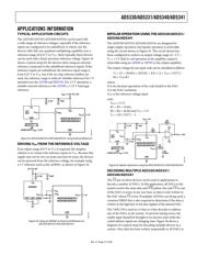
BIPOLAR OPERATION USING THE AD5330/AD5331/
AD5340/AD5341
The AD5330/AD5331/AD5340/AD5341 are designed for
single-supply operation, but bipolar operation is achievable
using the circuit shown in Figure 45. The circuit shown has
been configured to achieve an output voltage range of –5 V <
V
O
< +5 V. Rail-to-rail operation at the amplifier output is
achievable using an AD820 or OP295 as the output amplifier.
The output voltage for any input code can be calculated as follows:
V
O
= [(1 + R4/R3) × (R2/(R1 + R2) × (2 × V
REF
× D/2
N
)] –
R4 × V
REF
/R3
where:
D is the decimal equivalent of the code loaded to the DAC.
N is the DAC resolution.
V
REF
is the reference voltage input.
with:
V
REF
= 2.5 V.
R1 = R3 = 10 kΩ.
R2 = R4 = 20 kΩ and V
DD
= 5 V.
V
O
= (10 × D/2
N
) − 5.
V
DD
= 5
V
+
0.1µF 10µF
R2
20kΩ
R1
10kΩ
R3
10kΩ
R4
20kΩ
GND
V
O
= ±5V
+5V
–5V
AD5330/AD5331/
AD5340/AD5341
V
REF
V
OUT
V
DD
GND
EXT
REF
V
OUT
V
IN
AD780/REF192
WITH V
DD
= 5V
OR
AD589 WITH V
DD
= 2.5V
0.1µF
06852-046
Figure 45. Bipolar Operation using the AD5330/AD5331/AD5340/AD5341
DECODING MULTIPLE AD5330/AD5331/
AD5340/AD5341
The
CS
pin on these devices can be used in applications to
decode a number of DACs. In this application, all DACs in the
system receive the same data and
WR
pulses, but only
CS
to one
of the DACs is active at any one time, so data is only written to
the DAC whose
CS
is low. If multiple AD5341s are being used, a
common HBEN line is also required to determine if the data is
written to the high byte or low byte register of the selected DAC.
The 74HC139 is used as a 2-line to 4-line decoder to address
any of the DACs in the system. To prevent timing errors, the
enable input should be brought to its inactive state while the
coded address inputs are changing state. Figure 46 shows a
diagram of a typical setup for decoding multiple devices in a
system. Once data has been written sequentially to all DACs in
器件 Datasheet 文档搜索
AiEMA 数据库涵盖高达 72,405,303 个元件的数据手册,每天更新 5,000 多个 PDF 文件
