Datasheet 搜索 > DA转换器 > ADI(亚德诺) > AD5383BST-5 数据手册 > AD5383BST-5 数据手册 6/40 页

 器件3D模型
¥ 0
AD5383BST-5 数据手册 - ADI(亚德诺)
制造商:
ADI(亚德诺)
分类:
DA转换器
封装:
LQFP
描述:
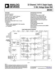
32通道, 14位,并行和串行输入,双极性电压输出DAC 32-Channel, 14-Bit, Parallel and Serial Input, Bipolar Voltage Output DAC
Pictures:
3D模型
符号图
焊盘图
引脚图
产品图
页面导航:
导航目录
AD5383BST-5数据手册
Page:
of 40 Go
若手册格式错乱,请下载阅览PDF原文件
AD5383
Rev. A | Page 6 of 40
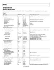
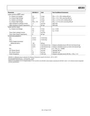
AD5383-3 SPECIFICATIONS
AV
DD
= 2.7 V to 3.6 V; DV
DD
= 2.7 V to 5.5 V, AGND = DGND = 0 V; external REFIN = 1.25 V; all specifications T
MIN
to T
MAX
, unless
otherwise noted.
Table 4.
Parameter AD5383-3
1
Unit Test Conditions/Comments
ACCURACY
Resolution 12 Bits
Relative Accuracy
2
(INL) ±1 LSB max
Differential Nonlinearity (DNL) ±1 LSB max Guaranteed monotonic over temperature
Zero-Scale Error 4 mV max
Offset Error ±4 mV max Measured at Code 64 in the linear region
Offset Error TC ±5 µV/°C typ
Gain Error ±0.024 % FSR max At 25°C
±0.1 % FSR max T
MIN
to T
MAX
Gain Temperature Coefficient
3
2 ppm FSR/°C typ
DC Crosstalk
3
0.5 LSB max
REFERENCE INPUT/OUTPUT
Reference Input
3
Reference Input Voltage 1.25 V ±1% for specified performance
DC Input Impedance 1 MΩ min Typically 100 MΩ
Input Current ±10 µA max Typically ±30 nA
Reference Range 1 to AV
DD
/2 V min/max
Reference Output
4
Enabled via CR8 in the AD5383 control register,
CR10 selects the reference voltage
Output Voltage 1.245/1.255 V min/max At ambient; optimized for 1.25 V operation; CR10 = 0
2.47/2.53 V min/max 2.5 V reference enabled; CR10 = 1
Reference TC ±10 ppm/°C typ Temperature range: +25°C to +85°C
±15 ppm/°C typ
Temperature range: −40°C to +85°C
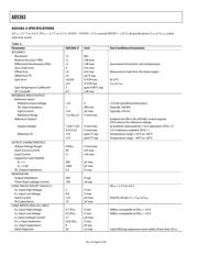
OUTPUT CHARACTERISTICS
3
Output Voltage Range
2
0/AV
DD
V min/max
Short-Circuit Current 40 mA max
Load Current ±1 mA max
Capacitive Load Stability
R
L
= ∞ 200 pF max
R
L
= 5 kΩ 1000 pF max
DC Output Impedance 0.5 Ω max
MONITOR PIN
Output Impedance 500 Ω typ
Three-State Leakage Current 100 nA typ
LOGIC INPUTS (EXCEPT SDA/SCL)
3
DV
DD
= 2.7 V to 3.6 V
V
IH
, Input High Voltage 2 V min
V
IL,
Input Low Voltage 0.8 V max
Input Current ±10 µA max Total for all pins; T
A
= T
MIN
to T
MAX
Pin Capacitance 10 pF max
LOGIC INPUTS (SDA, SCL ONLY)
V
IH
, Input High Voltage 0.7 DV
DD
V min SMBus-compatible at DV
DD
< 3.6 V
V
IL
, Input Low Voltage 0.3 DV
DD
V max SMBus-compatible at DV
DD
< 3.6 V
I
IN
, Input Leakage Current ±1 µA max
V
HYST
, Input Hysteresis 0.05 DV
DD
V min
C
IN
, Input Capacitance 8 pF typ
Glitch Rejection 50 ns max Input filtering suppresses noise spikes of less than 50 ns
器件 Datasheet 文档搜索
AiEMA 数据库涵盖高达 72,405,303 个元件的数据手册,每天更新 5,000 多个 PDF 文件
