Datasheet 搜索 > DA转换器 > ADI(亚德诺) > AD5683RBRMZ 数据手册 > AD5683RBRMZ 数据手册 6/29 页
 器件3D模型
¥ 6.877
AD5683RBRMZ 数据手册 - ADI(亚德诺)
制造商:
ADI(亚德诺)
分类:
DA转换器
封装:
MSOP-10
描述:
ANALOG DEVICES AD5683RBRMZ 数模转换器, 16 bit, 串行, 2.7V 至 5.5V, MSOP, 10 引脚
Pictures:
3D模型
符号图
焊盘图
引脚图
产品图
页面导航:
引脚图在P9P10P27Hot
典型应用电路图在P7
原理图在P1P3P19
封装尺寸在P27
型号编码规则在P28
功能描述在P1P9P10P27
技术参数、封装参数在P1P4P7P8
应用领域在P1
电气规格在P11
导航目录
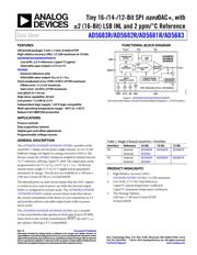
AD5683RBRMZ数据手册
Page:
of 29 Go
若手册格式错乱,请下载阅览PDF原文件

AD5683R/AD5682R/AD5681R/AD5683 Data Sheet
Rev. D | Page 6 of 28
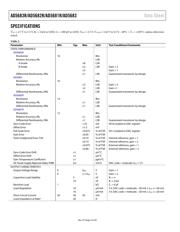
AC CHARACTERISTICS
V
DD
= 2.7 V to 5.5 V, R
L
= 2 kΩ to GND, C
L
= 200 pF to GND, V
REF
= 2.5 V, V
LOGIC
= 1.62 V to 5.5 V, −40°C < T
A
< +105°C, unless otherwise
noted.
1
Table 3.
Parameter Typ Max Unit Test Conditions/Comments
Output Voltage Settling Time
2, 3
5 7 µs Gain = 1
Slew Rate 0.7 V/µs
Digital-to-Analog Glitch Impulse
2
0.1 nV-sec ±1 LSB change around major carry, gain = 2
Digital Feedthrough
2
0.1 nV-sec
Total Harmonic Distortion
2
−83 dB V
REF
= 2 V ± 0.1 V p-p, frequency = 10 kHz
Output Noise Spectral Density 200 nV/√Hz DAC code = midscale, 10 kHz
Output Noise 6 µV p-p 0.1 Hz to 10 Hz; internal reference, DAC = zero scale
SNR 90 dB At ambient, BW = 20 kHz, V
DD
= 5 V, f
OUT
= 1 kHz
SFDR 88 dB At ambient, BW = 20 kHz, V
DD
= 5 V, f
OUT
= 1 kHz
SINAD 82 dB At ambient, BW = 20 kHz, V
DD
= 5 V, f
OUT
= 1 kHz
1
Temperature range = −40°C to +105°C, typical at 25°C.
2
See the Terminology section.
3
AD5683R/AD5683 to ±2 LSB, AD5682R to ±1 LSB, AD5681R to ±0.5 LSB.
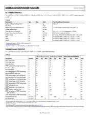
TIMING CHARACTERISTICS
V
DD
= 2.7 V to 5.5 V, V
LOGIC
= 1.62 V to 5.5 V, −40°C < T
A
< +105°C, unless otherwise noted.
Table 4.
Parameter
1
Symbol
1.62 V ≤ V
LOGIC
≤ 2.7 V 2.7 V ≤ V
LOGIC
2
≤ 5.5 V Daisy Chain and Readback
Unit
Min Typ Max Min Typ Max Min Typ Max
SCLK Cycle Time
t
1
33
20
40
ns
SCLK High Time t
2
16 10 20 ns
SCLK Low Time t
3
16 10 20 ns
SYNC
to SCLK Falling Edge Setup Time t
4
15
10
20 ns
Data Setup Time t
5
5 5 5 ns
Data Hold Time t
6
5 5 5 ns
SCLK Falling Edge to
SYNC
Rising Edge
t
7
15
10
10
ns
Minimum
SYNC
High Time t
8
20
20
40 ns
SYNC
Falling Edge to SCLK Fall Ignore t
9
16
10
10 ns
SDO Data Valid from SCLK Rising Edge t
10
35 ns
SYNC
Rising Edge to SCLK Falling Edge t
11
10 ns
SYNC
Rising Edge to SDO Disabled t
12
60 ns
SYNC
Rising Edge to
LDAC
Falling Edge t
13
25
25
25 ns
LDAC
Pulse Width Low t
14
20
15
15 ns
RESET
Minimum Pulse Width Low t
15
75
75
75 ns
RESET
Pulse Activation Time t
16
150
150
150 ns
SYNC
Rising Edge to
SYNC
Rising Edge
(DAC Updates)
t
17
1.9 1.7 1.7 µs
LDAC
Falling Edge to
SYNC
Rising Edge t
18
1.8 1.65 1.65 µs
Reference Power-Up
3
t
REF_POWER_UP
4
600 600 600 µs
Exit Shutdown
3
t
SHUTDOWN
5
6 6 6 µs
1
All input signals are specified with t
R
= t
F
= 1 ns/V (10% to 90% of V
DD
) and timed from a voltage level of (V
IL
+ V
IH
)/2.
2
Substitute V
DD
for V
LOGIC
on devices that do not include a V
LOGIC
pin.
3
Not shown in Figure 4.
4
Same timing must be expected when powering up the device after V
DD
= 2.7 V.
5
Time required to exit power-down to normal mode of AD5683R/AD5682R/AD5681R operation;
SYNC
rising edge to 90% of DAC midscale value, with output unloaded.
器件 Datasheet 文档搜索
AiEMA 数据库涵盖高达 72,405,303 个元件的数据手册,每天更新 5,000 多个 PDF 文件
