Datasheet 搜索 > AD转换器 > ADI(亚德诺) > AD7401YRWZ 数据手册 > AD7401YRWZ 数据手册 1/20 页
 器件3D模型
¥ 9.448
AD7401YRWZ 数据手册 - ADI(亚德诺)
制造商:
ADI(亚德诺)
分类:
AD转换器
封装:
SOIC-16
描述:
ANALOG DEVICES AD7401YRWZ 模数转换器, 16 bit, 16 MSPS, 3 V, 5.25 V, SOIC
Pictures:
3D模型
符号图
焊盘图
引脚图
产品图
页面导航:
导航目录
AD7401YRWZ数据手册
Page:
of 20 Go
若手册格式错乱,请下载阅览PDF原文件
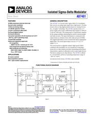
Isolated Sigma-Delta Modulator
Data Sheet
AD7401
Rev. E Document Feedback
Information furnished by Analog Devices is believed to be accurate and reliable. However, no
responsibility is assumed by Analog Devices for its use, nor for any infringements of patents or other
rights of third parties that may result from its use. Specifications subject to change without notice. No
license is granted by implication or otherwise under any patent or patent rights of Analog Devices.
Trademarks and registered trademarks are the property of their respective owners.
One Technology Way, P.O. Box 9106, Norwood, MA 02062-9106, U.S.A.
Tel: 781.329.4700 ©2006–2015 Analog Devices, Inc. All rights reserved.
Technical Support www.analog.com
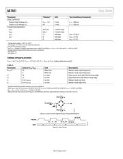
FEATURES
20 MHz maximum external clock rate
Second-order modulator
16 bits no missing codes
±2 LSB INL typical at 16 bits
3.5 μV/°C maximum offset drift
On-board digital isolator
On-board reference
Low power operation: 20 mA maximum at 5.25 V
−40°C to +105°C operating range
16-lead SOIC package
Safety and regulatory approvals
UL recognition
5000 V rms for 1 minute per UL 1577
CSA Component Acceptance Notice #5A
VDE Certificate of Conformity
DIN V VDE V 0884-10 (VDE V 0884-10):2006-12
V
IORM
= 891 V peak
APPLICATIONS
AC motor controls
Data acquisition systems
A/D + opto-isolator replacements
GENERAL DESCRIPTION
The AD7401
1
is a second-order, sigma-delta (Σ-Δ) modulator
that converts an analog input signal into a high speed, 1-bit data
stream with on-chip digital isolation based on Analog Devices,
Inc., iCoupler® technology. The AD7401 operates from a 5 V
power supply and accepts a differential input signal of ±200 mV
(±320 mV full scale). The analog input is continuously sampled
by the analog modulator, eliminating the need for external sample-
and-hold circuitry. The input information is contained in the
output stream as a density of ones with a data rate up to 20 MHz.
The original information can be reconstructed with an appropriate
digital filter. The serial input/output can use a 5 V or a 3 V
supply (V
DD2
).
The serial interface is digitally isolated. High speed CMOS,
combined with monolithic air core transformer technology,
means the on-chip isolation provides outstanding performance
characteristics, superior to alternatives such as optocoupler devices.
The device contains an on-chip reference. The AD7401 is offered
in a 16-lead SOIC and has an operating temperature range of
−40°C to +105°C.
An internal clock version, AD7400, is also available.
1
Protected by U.S. Patents 5,952,849; 6,873,065; and 7,075,329.
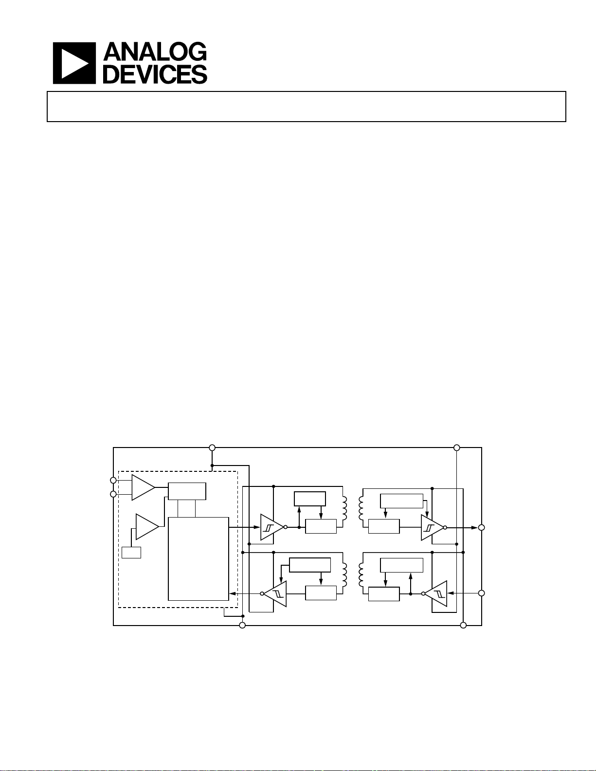
FUNCTIONAL BLOCK DIAGRAM
V
IN
+
V
DD1
V
DD2
V
IN
–
Σ-∆ ADC
CONTROL LOGIC
AD7401
B
U
F
T
/
H
REF
W ATCHDOG
GND
1
GND
2
MDAT
MCLKIN
DECODE
ENCODE DECODE
ENCODE
UPDATE
W ATCHDOG
UPDATE
05851-001
Figure 1.
器件 Datasheet 文档搜索
AiEMA 数据库涵盖高达 72,405,303 个元件的数据手册,每天更新 5,000 多个 PDF 文件
