Datasheet 搜索 > AD转换器 > ADI(亚德诺) > AD7686BRMZ 数据手册 > AD7686BRMZ 数据手册 12/28 页
 器件3D模型
¥ 134.937
AD7686BRMZ 数据手册 - ADI(亚德诺)
制造商:
ADI(亚德诺)
分类:
AD转换器
封装:
MSOP-10
描述:
ANALOG DEVICES AD7686BRMZ 模数转换器, SAR, 16 bit, 500 kSPS, 单, 1.8 V, 5.8 V, MSOP
Pictures:
3D模型
符号图
焊盘图
引脚图
产品图
页面导航:
导航目录
AD7686BRMZ数据手册
Page:
of 28 Go
若手册格式错乱,请下载阅览PDF原文件
AD7686 Data Sheet
THEORY OF OPERATION
SW+MSB
16,384C
IN+
LSB
COMP
CONTROL
LOGIC
SWITCHES CONTROL
BUSY
OUTPUT CODE
CNV
REF
GND
IN–
4C 2C C C32,768C
SW–MSB
16,384C
LSB
4C 2C C C32,768C
02969-024
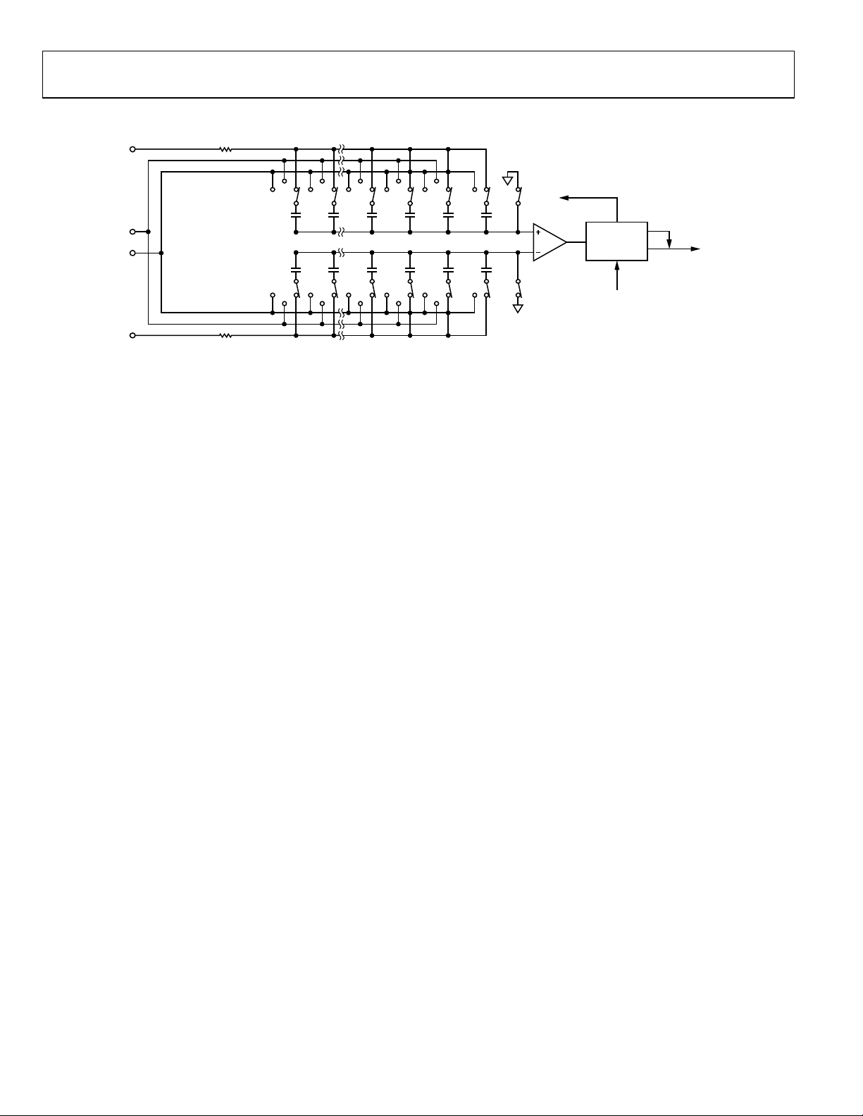
Figure 24. ADC Simplified Schematic
CIRCUIT INFORMATION
The AD7686 is a fast, low power, single-supply, precise 16-bit
ADC using a successive approximation architecture.
The AD7686 is capable of converting 500,000 samples per
second (500 kSPS) and powers down between conversions.
For example, when operating at 100 SPS, the device consumes
3.75 µW typically, which is ideal for battery-powered
applications.
The AD7686 provides the user with on-chip, track-and-hold
and does not exhibit any pipeline delay or latency, making it
ideal for multiple, multiplexed channel applications.
The AD7686 is specified from 4.5 V to 5.5 V and can be
interfaced to any of the 1.8 V to 5 V digital logic family. It is
housed in a 10-lead MSOP or a tiny 10-lead LFCSP that
combines space savings and allows flexible configurations.
This device is pin-for-pin-compatible with the AD7685,
AD7687, and AD7688.
CONVERTER OPERATION
The AD7686 is a successive approximation ADC based on a
charge redistribution DAC. Figure 24 shows a simplified
schematic of the ADC. The capacitive DAC consists of two
identical arrays of 16 binary weighted capacitors, which are
connected to two comparator inputs.
During the acquisition phase, terminals of the array tied to the
comparator input are connected to GND via SW+ and SW−.
All independent switches are connected to the analog inputs.
Therefore, the capacitor arrays are used as sampling capacitors
and acquire the analog signal on the IN+ and IN− inputs. When
the acquisition phase is complete and the CNV input goes high,
a conversion phase initiates. When the conversion phase begins,
SW+ and SW− are opened first.
The two capacitor arrays are then disconnected from the inputs
and connected to the GND input. Therefore, the differential
voltage between the inputs IN+ and IN−, captured at the end of
the acquisition phase, is applied to the comparator inputs,
causing the comparator to become unbalanced.
By switching each element of the capacitor array between GND
and REF, the comparator input varies by binary weighted
voltage steps (V
REF
/2, V
REF
/4 . . . V
REF
/65536). The control logic
toggles these switches, starting with the MSB, to bring the
comparator back into a balanced condition. After the
completion of this process, the part returns to the acquisition
phase and the control logic generates the ADC output code and
a busy signal indicator. Because the AD7686 has an on-board
conversion clock, the serial clock, SCK, is not required for the
conversion process.
Rev. C | Page 12 of 28
器件 Datasheet 文档搜索
AiEMA 数据库涵盖高达 72,405,303 个元件的数据手册,每天更新 5,000 多个 PDF 文件
