Datasheet 搜索 > AD转换器 > ADI(亚德诺) > AD7686BRMZ 数据手册 > AD7686BRMZ 数据手册 7/28 页
 器件3D模型
¥ 134.937
AD7686BRMZ 数据手册 - ADI(亚德诺)
制造商:
ADI(亚德诺)
分类:
AD转换器
封装:
MSOP-10
描述:
ANALOG DEVICES AD7686BRMZ 模数转换器, SAR, 16 bit, 500 kSPS, 单, 1.8 V, 5.8 V, MSOP
Pictures:
3D模型
符号图
焊盘图
引脚图
产品图
页面导航:
导航目录
AD7686BRMZ数据手册
Page:
of 28 Go
若手册格式错乱,请下载阅览PDF原文件
Data Sheet AD7686
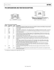
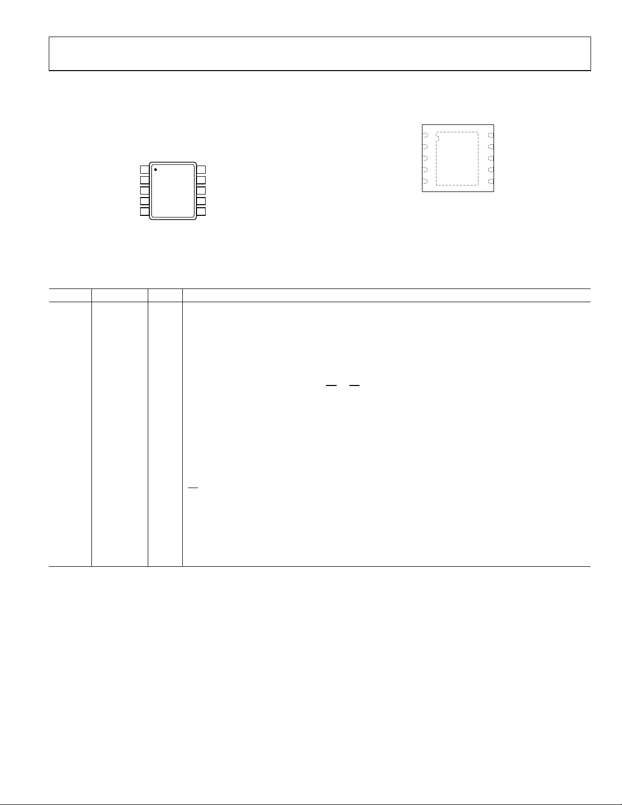
PIN CONFIGURATIONS AND FUNCTION DESCRIPTIONS
02969-005
REF
1
VDD
2
IN+
3
IN–
4
GND
5
VIO
10
SDI
9
SCK
8
SDO
7
CNV
6
AD7686
T
O
P VIEW
(Not to Scale)
Figure 5. 10-Lead MSOP Pin Configuration
02969-006
1REF
2VDD
3IN+
4IN–
5GND
10 VIO
9
SDI
8 SCK
7
SDO
6
CNV
AD7686
TOP VIEW
(Not to Scale)
NOTES
1.EXPOSED PAD. THE EXPOSED PAD MUST BE CONNECTED
TO GROUND. THIS CONNECTION IS NOT REQUIRED TO
MEET ELECTRICAL PERFORMANCES.
Figure 6. 10-Lead LFCSP Pin Configuration
Table 6. Pin Function Descriptions
Pin No. Mnemonic Type
1
Description
1 REF AI Reference Input Voltage. The REF range is from 0.5 V to VDD. It is referred to the GND pin. This pin should
be decoupled closely to the pin with a 10 µF capacitor.
2 VDD P Power Supply.
3 IN+ AI Analog Input. It is referred to IN−. The voltage range, that is, the difference between IN+ and IN−, is 0 V to V
REF
.
4 IN− AI Analog Input Ground Sense. It is connected to the analog ground plane or to a remote sense ground.
5 GND P Power Supply Ground.
6 CNV DI Convert Input. This input has multiple functions. On its leading edge, it initiates the conversions and
selects the interface mode, chain, or
CS
. In
CS
mode, it enables the SDO pin when low. In chain mode,
the data should be read when CNV is high.
7
SDO
DO
Serial Data Output. The conversion result is output on this pin. It is synchronized to SCK.
8
SCK
DI
Serial Data Clock Input. When the part is selected, the conversion result is shifted out by this clock.
9 SDI DI Serial Data Input. This input provides multiple features. It selects the interface mode of the ADC as
follows:
Chain mode is selected if SDI is low during the CNV rising edge. In this mode, SDI is used as a data
input to daisy-chain the conversion results of two or more ADCs onto a single SDO line. The digital
data level on SDI is output on SDO with a delay of 16 SCK cycles.
CS
mode is selected if SDI is high during the CNV rising edge. In this mode, either SDI or CNV can
enable the serial output signals when low. If SDI or CNV is low when the conversion is completed,
the busy indicator feature is enabled.
10 VIO P Input/Output Interface Digital Power. Nominally at the same supply as the host interface (1.8 V, 2.5 V,
3 V, or 5 V).
EPAD N/A Exposed Pad. The exposed pad must be connected to ground. This connection is not required to meet
electrical performances.
1
AI = analog input, DI = digital input, DO = digital output, and P = power.
Rev. C | Page 7 of 28
器件 Datasheet 文档搜索
AiEMA 数据库涵盖高达 72,405,303 个元件的数据手册,每天更新 5,000 多个 PDF 文件
