Datasheet 搜索 > AD转换器 > ADI(亚德诺) > AD7715ARZ-5REEL 数据手册 > AD7715ARZ-5REEL 数据手册 10/40 页
 器件3D模型
¥ 43.403
AD7715ARZ-5REEL 数据手册 - ADI(亚德诺)
制造商:
ADI(亚德诺)
分类:
AD转换器
封装:
SOIC-16
描述:
3 V / 5 V , 450 MUA 16位Σ-Δ型ADC 3 V/5 V, 450 muA 16-Bit, Sigma-Delta ADC
Pictures:
3D模型
符号图
焊盘图
引脚图
产品图
页面导航:
导航目录
AD7715ARZ-5REEL数据手册
Page:
of 40 Go
若手册格式错乱,请下载阅览PDF原文件
AD7715 Data Sheet
Rev. E | Page 10 of 40
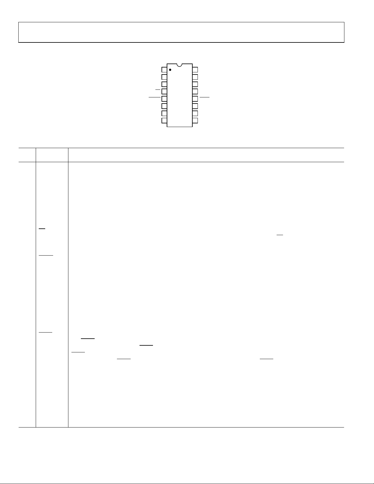
PIN CONFIGURATION AND FUNCTION DESCRIPTIONS
14
13
12
11
16
15
10
9
8
1
2
3
4
7
6
5
TOP VIEW
(Not to Scale)
AD7715
SCLK
DOUT
DIN
DV
DD
DGND
MCLK IN
MCLK OUT
CS
REF IN(+)
AGND
DRDY
RESET
AV
DD
AIN(+)
AIN(–)
REF IN(–)
08519-003
Figure 3. Pin Configuration
Table 6. Pin Function Descriptions
Pin
No. Mnemonic Description
1 SCLK Serial Clock. Logic input. An external serial clock is applied to this input to access serial data from the AD7715. This
serial clock can be a continuous clock with all data transmitted in a continuous train of pulses. Alternatively, it can be a
noncontinuous clock with the information being transmitted to the AD7715 in smaller batches of data.
2 MCLK IN Master Clock Signal for the Device. This can be provided in the form of a crystal/resonator or external clock. A
crystal/resonator can be tied across the MCLK IN and MCLK OUT pins. Alternatively, the MCLK IN pin can be driven
with a CMOS-compatible clock and MCLK OUT left unconnected. The part is specified with clock input frequencies of
both 1 MHz and 2.4576 MHz.
3
MCLK OUT
When the master clock for the device is a crystal/resonator, the crystal/resonator is connected between MCLK IN and
MCLK OUT. If an external clock is applied to MCLK IN, MCLK OUT provides an inverted clock signal. This clock can be
used to provide a clock source for external circuitry.
4
CS
Chip Select. Active low logic input used to select the AD7715. With this input hardwired low, the AD7715 can operate
in its three-wire interface mode with SCLK, DIN, and DOUT used to interface to the device.
CS
can be used to select
the device in systems with more than one device on the serial bus or as a frame synchronization signal in
communicating with the AD7715.
5
RESET
Logic Input. Active low input which resets the control logic, interface logic, calibration coefficients, digital filter, and
analog modulator of the part to power-on status.
6 AV
DD
Analog Positive Supply Voltage, 3.3 V nominal (AD7715-3) or 5 V nominal (AD7715-5).
7 AIN(+) Analog Input. Positive input of the programmable gain differential analog input to the AD7715.
8 AIN(−) Analog Input. Negative input of the programmable gain differential analog input to the AD7715.
9 REF IN(+) Reference Input. Positive input of the differential reference input to the AD7715. The reference input is differential
with the provision that REF IN(+) must be greater than REF IN(–). REF IN(+) can lie anywhere between AV
DD
and AGND.
10 REF IN(−) Reference Input. Negative input of the differential reference input to the AD7715. The REF IN(−) can lie anywhere
between AV
DD
and AGND provided REF IN(+) is greater than REF IN(–).
11 AGND Ground Reference Point for Analog Circuitry. For correct operation of the AD7715, no voltage on any of the other pins
should go more than 30 mV negative with respect to AGND.
12
DRDY
Logic Output. A logic low on this output indicates that a new output word is available from the AD7715 data register.
The
DRDY
pin returns high upon completion of a read operation of a full output word. If no data read has taken place
between output updates, the
DRDY
line returns high for 500 × t
CLK IN
cycles prior to the next output update. While
DRDY
is high, a read operation should not be attempted or in progress to avoid reading from the data register as it is
being updated. The
DRDY
line returns low again when the update has taken place.
DRDY
is also used to indicate when
the AD7715 has completed its on-chip calibration sequence.
13 DOUT Serial data output with serial data being read from the output shift register on the part. This output shift register can
contain information from the setup register, communications register or data register depending on the register
selection bits of the communications register.
14 DIN Serial data input
with serial data being written to the input shift register on the part. Data from this input shift register
is transferred to the setup register or communications register depending on the register selection bits of the
communications register.
15 DV
DD
Digital Supply Voltage, 3.3 V or 5 V nominal.
16 DGND Ground reference point for digital circuitry.
器件 Datasheet 文档搜索
AiEMA 数据库涵盖高达 72,405,303 个元件的数据手册,每天更新 5,000 多个 PDF 文件
