Datasheet 搜索 > AD转换器 > ADI(亚德诺) > AD7715ARZ-5REEL 数据手册 > AD7715ARZ-5REEL 数据手册 7/40 页
 器件3D模型
¥ 43.403
AD7715ARZ-5REEL 数据手册 - ADI(亚德诺)
制造商:
ADI(亚德诺)
分类:
AD转换器
封装:
SOIC-16
描述:
3 V / 5 V , 450 MUA 16位Σ-Δ型ADC 3 V/5 V, 450 muA 16-Bit, Sigma-Delta ADC
Pictures:
3D模型
符号图
焊盘图
引脚图
产品图
页面导航:

导航目录
AD7715ARZ-5REEL数据手册
Page:
of 40 Go
若手册格式错乱,请下载阅览PDF原文件
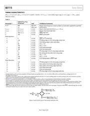
Data Sheet AD7715
Rev. E | Page 7 of 40
AV
DD
= 3 V to 5 V, DV
DD
= 3 V to 5 V, REF IN(+) = 1.25 V (AD7715-3) or 2.5 V (AD7715-5); REF IN(−) = AGND; MCLK IN = 1 MHz to
2.4576 MHz, unless otherwise noted. All specifications T
MIN
to T
MAX
, unless otherwise noted.
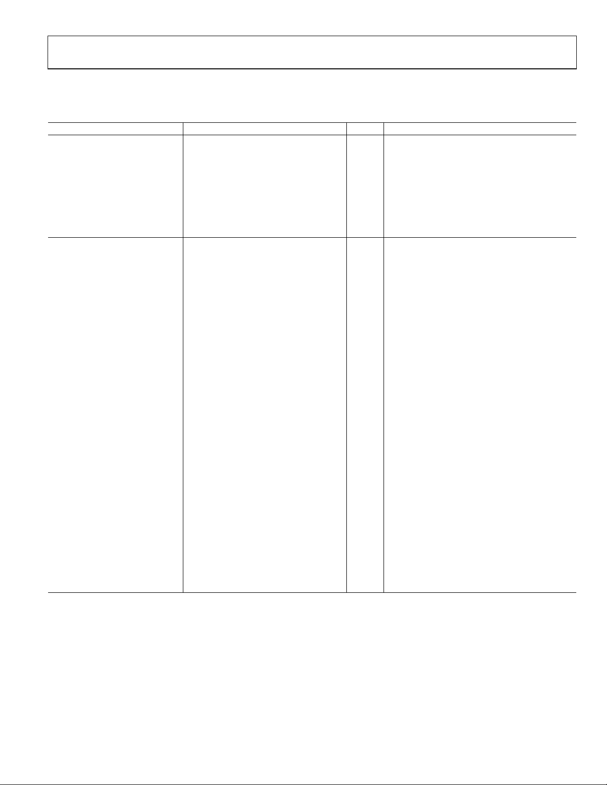
Table 3.
Parameter
Min
Typ
Max
Unit Conditions/Comments
SYSTEM CALIBRATION
Positive Full-Scale Calibration Limit
1
(1.05 ×
V
REF
)/GAIN
V GAIN Is the selected PGA gain (1, 2, 32, or 128)
Negative Full-Scale Calibration Limit
1
−(1.05 ×
V
REF
)/GAIN
V GAIN Is the selected PGA gain (1, 2, 32, or 128)
Offset Calibration Limit
2
−(1.05 ×
V
REF
)/GAIN
V GAIN Is the selected PGA gain (1, 2, 32, or 128)
Input Span
2
0.8 ×
V
REF
/GAIN
V GAIN Is the selected PGA gain (1, 2, 32, or 128)
(2.1 × V
REF
)/GAIN V GAIN Is the selected PGA gain (1, 2, 32, or 128)
POWER REQUIREMENTS
Power Supply Voltages
AV
DD
Voltage (AD7715-3) 3 3.6 V For specified performance
AV
DD
Voltage (AD7715-5) 4.75 5.25 V For specified performance
DV
DD
Voltage 3 5.25 V For specified performance
Power Supply Currents
AV
DD
Current
AV
DD
= 3.3 V or 5 V. gain = 1 to 128 (f
CLK IN
= 1 MHz) or
gain = 1 or 2 (f
CLK IN
= 2.4576 MHz)
0.27 mA Typically 0.2 mA; BUF bit of the setup register = 0
0.6 mA
Typically 0.4 mA; BUF bit of the setup register = 1, AV
DD
= 3.3 V or 5 V; gain = 32 or 128 (f
CLK IN
= 2.4576 MHz)
3
0.5 mA Typically 0.3 mA; BUF bit of the setup register = 0
1.1 mA Typically 0.8 mA; BUF bit of the setup register = 1
DV
DD
Current
4
Digital inputs = 0 V or DV
DD
; external MCLK IN
0.18 mA Typically 0.15 mA. DV
DD
= 3.3 V. f
CLK IN
= 1 MHz
0.4 mA Typically 0.3 mA. DV
DD
= 5 V. f
CLK IN
= 1 MHz
0.5 mA Typically 0.4 mA. DV
DD
= 3.3 V. f
CLK IN
= 2.4576 MHz
0.8
mA
Typically 0.6 mA. DV
DD
= 5 V. f
CLK IN
= 2.4576 MHz
Power Supply Rejection
5
Depends on gain
6
dB
Normal-Mode Power Dissipation
4
AV
DD
= DV
DD
= 3.3 V; digital inputs = 0 V or DV
DD
; external
MCLK IN
1.5 mW BUF bit = 0. all gains 1 MHz clock
2.65 mW BUF bit = 1. all gains 1 MHz clock
3.3 mW BUF bit = 0. Gain = 32 or 128 @ f
CLK IN
= 2.4576 MHz
5.3 mW BUF bit = 1. Gain = 32 or 128 @ f
CLK IN
= 2.4576 MHz
Normal-Mode Power Dissipation
4
AV
DD
= DV
DD
= 5 V. digital inputs = 0 V or DV
DD
; external
MCLK IN
3.25 mW BUF bit = 0; all gains 1 MHz clock
5 mW BUF bit = 1; all gains 1 MHz clock
6.5 mW BUF bit = 0; gain = 32 or 128 @ f
CLK IN
= 2.4576 MHz
9.5 mW BUF bit = 1; gain = 32 or 128 @ f
CLK IN
= 2.4576 MHz
Standby (Power-Down) Current
7
20 µA External MCLK IN = 0 V or DV
DD
. typically 10 µA; V
DD
= 5 V
Standby (Power-Down) Current
7
10 µA External MCLK IN = 0 V or DV
DD
. typically 5 µA; V
DD
= 3.3 V
1
After calibration, if the analog input exceeds positive full scale, the converter outputs all 1s. If the analog input is less than negative full scale, then the device outputs
all 0s.
2
These calibration and span limits apply provided the absolute voltage on the analog inputs does not exceed AV
DD
+ 30 mV or go more negative than AGND − 30 mV.
The offset calibration limit applies to both the unipolar zero point and the bipolar zero point.
3
Assumes CLK Bit of setup register is set to correct status corresponding to the master clock frequency.
4
When using a crystal or ceramic resonator across the MCLK pins as the clock source for the device, the DV
DD
current and power dissipation will vary depending on the
crystal or resonator type (see the Clocking and Oscillator Circuit section).
5
Measured at dc and applies in the selected pass-band. PSRR at 50 Hz exceeds 120 dB with filter notches of 25 Hz or 50 Hz. PSRR at 60 Hz exceeds 120 dB with filter
notches of 20 Hz or 60 Hz.
6
PSRR depends on gain. Gain of 1:85 dB typical; gain of 2:90 dB typical; gains of 32 and 128:95 dB typical.
7
If the external master clock continues to run in standby mode, the standby current increases to 50 µA typical. When using a crystal or ceramic resonator across the
MCLK pins as the clock source for the device, the internal oscillator continues to run in standby mode and the power dissipation depends on the crystal or resonator
type (see the Standby Mode section).
器件 Datasheet 文档搜索
AiEMA 数据库涵盖高达 72,405,303 个元件的数据手册,每天更新 5,000 多个 PDF 文件
