Datasheet 搜索 > ADI(亚德诺) > AD7782 数据手册 > AD7782 数据手册 1/12 页


¥ 0
AD7782 数据手册 - ADI(亚德诺)
制造商:
ADI(亚德诺)
描述:
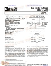
只读,引脚配置的24位ADC Read Only, Pin Configured 24-Bit ADC
Pictures:
3D模型
符号图
焊盘图
引脚图
产品图
页面导航:
导航目录
AD7782数据手册
Page:
of 12 Go
若手册格式错乱,请下载阅览PDF原文件
REV. 0
Information furnished by Analog Devices is believed to be accurate and
reliable. However, no responsibility is assumed by Analog Devices for its
use, nor for any infringements of patents or other rights of third parties that
may result from its use. No license is granted by implication or otherwise
under any patent or patent rights of Analog Devices.
a
AD7782
One Technology Way, P.O. Box 9106, Norwood, MA 02062-9106, U.S.A.
Tel: 781/329-4700www.analog.com
Fax: 781/326-8703 © Analog Devices, Inc., 2001
Read Only, Pin Configured
24-Bit ⌺-⌬ ADC
FEATURES
2-Channel, 24-Bit ⌺-⌬ ADC
Pin Configurable (No Programmable Registers)
Pin Selectable Input Channels
Pin Programmable Input Ranges (ⴞ2.56 V or ⴞ160 mV)
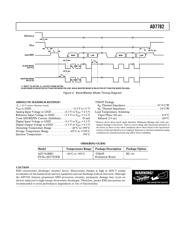
Fixed 19.79 Hz Update Rate
Simultaneous 50 Hz and 60 Hz Rejection
24-Bit No Missing Codes
18.5-Bit p-p Resolution (ⴞ2.56 V Range)
16.5-Bit p-p Resolution (ⴞ160 mV Range)
INTERFACE
Master or Slave Mode of Operation
Slave Mode
3-Wire Serial
SPI™, QSPI™, MICROWIRE™, and DSP-Compatible
Schmitt Trigger on SCLK
POWER
Specified for Single 3 V and 5 V Operation
Normal: 1.3 mA @ 3 V
Power-Down: 9 A
ON-CHIP FUNCTIONS
Rail-Rail Input Buffer and PGA
APPLICATIONS
Sensor Measurement
Industrial Process Control
Temperature Measurement
Pressure Measurements
Weigh Scales
Portable Instrumentation
GENERAL DESCRIPTION
The AD7782 is a complete analog front end for low-frequency
measurement applications. The 24-bit sigma-delta ADC contains
two fully differential analog input channels that can be config-
ured with a gain of 1 or 16 allowing full-scale input signal ranges
of ±2.56 V or ±160 mV from a +2.5 V differential reference
input.
The AD7782 has an extremely simple, read-only digital interface
which can be operated in master mode or slave mode. There are
no on-chip registers to be programmed. The input signal range
and input channel selection are configured using two external pins.
SPI and QSPI are trademarks of Motorola Inc.
MICROWIRE is a trademark of National Semiconductor Corporation.
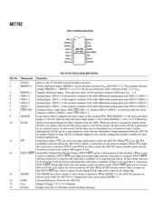
FUNCTIONAL BLOCK DIAGRAM
AIN1(+)
AIN1(–)
AIN2(+)
AIN2(–)
CH1/CH2 RANGE
AD7782
V
DD
GND
BUF PGA
REFIN(–)
REFIN(+)
MUX
24-BIT ⌺-⌬
ADC
OSCILLATOR
AND
PLL
DOUT/RDY
SCLK
MODE
XTAL1
XTAL2
SERIAL
INTERFACE
AND
CONTROL
LOGIC
CS
BASIC CONNECTION DIAGRAM
AD7782
REFIN(+)
REFIN(–)
AIN1(–)
AIN1(+)
AIN2(–)
AIN2(+)
XTAL1
V
DD
DOUT/RDY
CS
SCLK
XTAL2
GND
REFERENCE
INPUT
ANALOG
INPUT
ANALOG
INPUT
POWER SUPPLY
32.768kHz
CRYSTAL
DIGITAL
INTERFACE
The device operates from a 32.768 kHz crystal with an on-chip PLL
generating the required internal operating frequency. The output
data rate from the part is fixed via the master clock at 19.79 Hz and
provides simultaneous 50 Hz and 60 Hz rejection at this update
rate. Eighteen-bit p-p resolution can be obtained at this update rate.
The part operates from a single 3 V or 5 V supply. When operating
from 3 V supplies, the power dissipation for the part is 3.9 mW.
The AD7782 is available in a 16-lead TSSOP package.
Another part in the AD778x family is the AD7783. It is similar
to the AD7782 except it has two integrated current sources and
only one differential input channel.
查询AD7782BRU供应商 捷多邦,专业PCB打样工厂,24小时加急出货
器件 Datasheet 文档搜索
AiEMA 数据库涵盖高达 72,405,303 个元件的数据手册,每天更新 5,000 多个 PDF 文件
