Datasheet 搜索 > ADI(亚德诺) > AD7782 数据手册 > AD7782 数据手册 6/12 页


¥ 0
AD7782 数据手册 - ADI(亚德诺)
制造商:
ADI(亚德诺)
描述:
只读,引脚配置的24位ADC Read Only, Pin Configured 24-Bit ADC
Pictures:
3D模型
符号图
焊盘图
引脚图
产品图
页面导航:
导航目录
AD7782数据手册
Page:
of 12 Go
若手册格式错乱,请下载阅览PDF原文件
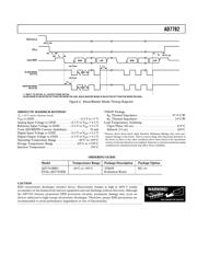
REV. 0
AD7782
–6–
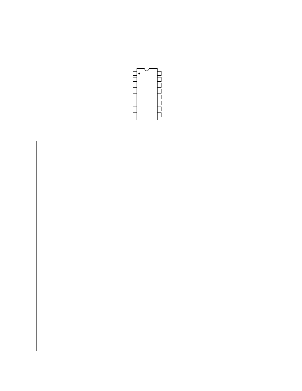
PIN CONFIGURATION
TOP VIEW
(Not to Scale)
XTAL1
AD7782
REFIN(+)
REFIN(–)
AIN1(+)
AIN1(–)
AIN2(+)
AIN2(–)
CH1/CH2
XTAL2
V
DD
GND
MODE
DOUT/RDY
CS
SCLK
RANGE
1
2
3
4
5
6
7
8
16
15
14
13
12
11
10
9
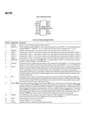
PIN FUNCTION DESCRIPTIONS
Pin No. Mnemonic Function
1 XTAL1 Input to the 32.768 kHz Crystal Oscillator Inverter.
2 REFIN(+) Positive Reference Input. REFIN(+) can lie anywhere between V
DD
and GND +1 V. The nominal reference
voltage (REFIN(+) – REFIN(–)) is 2.5 V, but the part functions with a reference from 1 V to V
DD
.
3 REFIN(–) Negative Reference Input. This reference input can lie anywhere between GND and V
DD
– 1 V.
4 AIN1(+) Analog Input. AIN1(+) is the positive terminal of the fully-differential analog input pair AIN1(+)/AIN1(–).
5 AIN1(–) Analog Input. AIN1(–) is the negative terminal of the fully-differential analog input pair AIN1(+)/AIN1(–).
6 AIN2(+) Analog Input. AIN2(+) is the positive terminal of the fully-differential analog input pair AIN2(+)/AIN2(–).
7 AIN2(–) Analog Input. AIN2(–) is the negative terminal of the fully-differential analog input pair AIN2(+)/AIN2(–).
8 CH1/CH2 Channel Select, Logic Input. With CH1/CH2 = 0, channel AIN1(+)/AIN1(–) is selected while the active
channel is AIN2(+)/AIN2(–) when CH1/CH2 = 1.
9 RANGE Logic Input which configures the input range on the internal PGA. With RANGE = 0, the full-scale input
range is ±160 mV while the full-scale input range equals ±2.56 V when RANGE = 1 for a +2.5 V Reference.
10 SCLK Serial Clock Input/Output for Data Transfers from the ADC. When the device is operated in master mode,
SCLK is an output with one SCLK period equal to one XTAL period. In slave mode, SCLK is generated
by an external source. In slave mode, all the data can be transmitted on a continuous train of pulses.
Alternatively, SCLK can be a noncontinuous clock with the information being transmitted from the AD7782
in smaller batches of data. SCLK is Schmitt triggered (slave mode) making the interface suitable for opto-
isolated applications.
11 CS Chip Select Input. CS is an active low logic input used to select the AD7782. When CS is low, the PLL
establishes lock and allows the AD7782 to initiate a conversion on the selected channel. When CS is high,
the conversion is aborted, DOUT and SCLK are three-stated, the AD7782 enters standby mode and any
conversion result in the output shift register is lost.
12 DOUT/RDY Serial Data Output/Data Ready Output. DOUT/RDY serves a dual purpose in this interface. When a con-
version is initiated, DOUT/RDY goes high and remains high until the conversion is complete. DOUT/RDY
will then return low to indicate that valid data is available to be read from the device. In slave mode, this acts
as an interrupt to the processor indicating that valid data is available. If data is not read after a conversion,
DOUT/RDY will go high before the next update occurs. In master mode, DOUT/RDY goes low for at least
half an SCLK cycle before the device produces SCLKs. When SCLK becomes active, data is output on
the DOUT/RDY pin. Data is output on the falling SCLK edge and is valid on the rising edge.
13 MODE The MODE pin selects master or slave mode of operation. When MODE = 0, the AD7782 operates in
master mode while the AD7782 is configured for slave mode when MODE = 1.
14 GND Ground Reference Point for the AD7782.
15 V
DD
Supply Voltage, 3 V or 5 V Nominal.
16 XTAL2 Output from the 32.768 kHz Crystal Oscillator Inverter.
器件 Datasheet 文档搜索
AiEMA 数据库涵盖高达 72,405,303 个元件的数据手册,每天更新 5,000 多个 PDF 文件
