Datasheet 搜索 > 时钟信号器件 > ADI(亚德诺) > AD9548BCPZ-REEL7 数据手册 > AD9548BCPZ-REEL7 数据手册 38/111 页
 器件3D模型
¥ 335.88
AD9548BCPZ-REEL7 数据手册 - ADI(亚德诺)
制造商:
ADI(亚德诺)
分类:
时钟信号器件
封装:
LFCSP-88
描述:
四路/八路输入网络时钟发生器/同步器 Quad/Octal Input Network Clock Generator/Synchronizer
Pictures:
3D模型
符号图
焊盘图
引脚图
产品图
页面导航:
引脚图在P15P33P51P111Hot
典型应用电路图在P46P51
原理图在P1P26P31P35P38P39P43
封装尺寸在P111
型号编码规则在P111
功能描述在P1P15P37P111
技术参数、封装参数在P1P4P8P10P11P14P106
应用领域在P1P37
电气规格在P18
导航目录
AD9548BCPZ-REEL7数据手册
Page:
of 111 Go
若手册格式错乱,请下载阅览PDF原文件
AD9548 Data Sheet
2×
÷N
VCO
CALIBRATION
LOCK
DETECT
SYSTEM
CLOCK
÷M
LOOP
FILTER
SYSCLKN
SYSCLKP
SYSCLK_VREG SYSCLK_LF
HF
XTAL
LF
48
52
53
49
PFD
AND
CHARGE
PUMP
08022-020
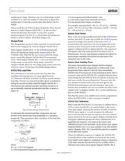
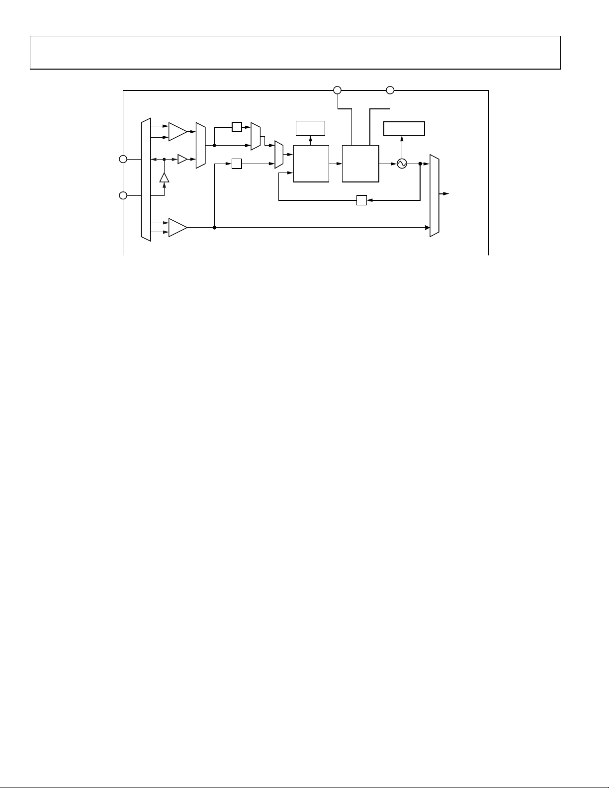
Figure 47. System Clock Block Diagram
System Clock Details
A block diagram of the system clock appears in Figure 47. The
signal at the SYSCLKx input pins becomes the internally buffered
DAC sampling clock (f
S
) via one of three paths.
• High frequency direct (HF)
• Low frequency synthesized (LF)
• Crystal resonator synthesized (XTAL)
Note that both the LF and XTAL paths require the use of the
SYSCLK PLL (see the SYSCLK PLL Multiplier section).
The main purpose of the HF path is to allow the direct use of a high
frequency (500 MHz to 1 GHz) external clock source for clocking
the AD9548. This path is optimized for high frequency and low
noise floor. Note that the HF input also provides a path to SYSCLK
PLL (see the SYSCLK PLL Multiplier section), which includes
an input divider (M) programmable for divide-by -1, -2, -4, or -8.
The purpose of the divider is to limit the frequency at the input
to the PLL to less than 150 MHz (the maximum PFD rate).
The LF path permits the user to provide an LVPECL, LVDS,
CMOS, or sinusoidal low frequency clock for multiplication by
the integrated SYSCLK PLL. The LF path handles input
frequencies from 3.5 MHz up to 100 MHz. However, when
using a sinusoidal input signal, it is best to use a frequency in
excess of 20 MHz. Otherwise, the resulting low slew rate can
lead to substandard noise performance. Note that the LF path
includes an optional 2× frequency multiplier to double the rate
at the input to the SYSCLK PLL and potentially reduce the PLL
in-band noise. However, to avoid exceeding the maximum PFD
rate of 150 MHz, using the 2× frequency multiplier is valid only
for input frequencies below 125 MHz.
The XTAL path enables the connection of a crystal resonator
(typically 10 MHz to 50 MHz) across the SYSCLKx input pins.
An internal amplifier provides the negative resistance required
to induce oscillation. The internal amplifier expects a 3.2 mm ×
2.5 mm AT cut, fundamental mode crystal with a maximum
motional resistance of 100 Ω. The following crystals, listed in
alphabetical order, may meet these criteria. Note that, whereas
these crystals may meet the preceding criteria according to their
data sheets, Analog Devices, Inc., does not guarantee their
operation with the AD9548, nor does Analog Devices endorse
one crystal manufacturer/supplier over another.
• AVX/Kyocera CX3225SB
• ECS ECX-32
• Epson/Toyocom TSX-3225
• Fox FX3225BS
• NDK NX3225SA
• Siward SX-3225
SYSCLK PLL MULTIPLIER
The SYSCLK PLL multiplier is an integer-N design and relies on
an integrated LC tank and VCO. It provides a means to convert
a low frequency clock input to the desired system clock
frequency, f
S
(900 MHz to 1 GHz). The SYSCLK PLL multiplier
accepts input signals between 3.5 MHz and 500 MHz, but
frequencies in excess of 150 MHz require the M-divider to
ensure compliance with the maximum PFD rate (150 MHz).
The PLL contains a feedback divider (N) that is programmable
for divide values between 6 and 255. The nominal VCO gain is
70 M H z / V.
Lock Detector
The SYSCLK PLL has a built-in lock detector. Register 0x0100,
Bit 2 determines whether the lock detector is active. When
active (default), the user controls the sensitivity of the lock
detector via the lock detect divider bits (Register 0x0100, Bits[1:0]).
Note that 0 must be written to the system clock stability timer
(Register 0x0106 to Register 0x0108) whenever the lock
detector is disabled (Register 0x0100, Bit 2 = 1).
The SYSCLK PLL phase detector operates at the PFD rate,
which is f
VCO
/N. Each PFD sample indicates whether the
reference and feedback signals are phase aligned (within a
certain threshold range).
While the PLL is in the process of acquiring a lock condition,
the PFD samples typically consist of an arbitrary sequence of
in-phase and out-of-phase indications. As the PLL approaches
complete phase lock, the number of consecutive in-phase PFD
Rev. G | Page 38 of 111
器件 Datasheet 文档搜索
AiEMA 数据库涵盖高达 72,405,303 个元件的数据手册,每天更新 5,000 多个 PDF 文件
