Datasheet 搜索 > 时钟信号器件 > ADI(亚德诺) > AD9548BCPZ-REEL7 数据手册 > AD9548BCPZ-REEL7 数据手册 5/111 页
 器件3D模型
¥ 335.88
AD9548BCPZ-REEL7 数据手册 - ADI(亚德诺)
制造商:
ADI(亚德诺)
分类:
时钟信号器件
封装:
LFCSP-88
描述:
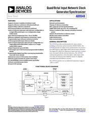
四路/八路输入网络时钟发生器/同步器 Quad/Octal Input Network Clock Generator/Synchronizer
Pictures:
3D模型
符号图
焊盘图
引脚图
产品图
页面导航:
引脚图在P15P33P51P111Hot
典型应用电路图在P46P51
原理图在P1P26P31P35P38P39P43
封装尺寸在P111
型号编码规则在P111
功能描述在P1P15P37P111
技术参数、封装参数在P1P4P8P10P11P14P106
应用领域在P1P37
电气规格在P18
导航目录
AD9548BCPZ-REEL7数据手册
Page:
of 111 Go
若手册格式错乱,请下载阅览PDF原文件
Data Sheet AD9548
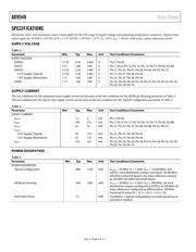
Parameter Min Typ Max Unit Test Conditions/Comments
Incremental Power Dissipation
Conditions = typical configuration; table values show the
change in power due to the indicated operation.
SYSCLK PLL Off −105 mW f
SYSCLK
= 1 GHz
1
; high frequency direct input mode.
Input Reference On
Differential 7 mW
Single-Ended 13 mW
Output Distribution Driver On
LVDS 70 mW
LVPECL 75 mW
CMOS 65 mW A single 3.3 V CMOS output with a 10 pF load.
1
f
SYSCLK
is the frequency at the SYSCLKP and SYSCLKN pins.
2
f
S
is the sample rate of the output DAC.
3
f
DDS
is the output frequency of the DDS.
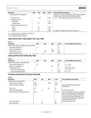
LOGIC INPUTS (M7 TO M0, RESET, TDI, TCLK, TMS)
Table 4.
Parameter Min Typ Max Unit Test Conditions/Comments
LOGIC INPUTS (M7 to M0, RESET, TDI, TCLK, TMS)
Input High Voltage (V
IH
) 2.1 V
Input Low Voltage (V
IL
) 0.8 V
Input Current (I
INH
, I
INL
)
±80
±200
µA
Input Capacitance (C
IN
) 3 pF
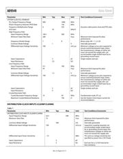
LOGIC OUTPUTS (M7 TO M0, IRQ, TDO)
Table 5.
Parameter Min Typ Max Unit Test Conditions/Comments
LOGIC OUTPUTS (M7 to M0, IRQ, TDO)
Output High Voltage (V
OH
) 2.7 V I
OH
= 1 mA
Output Low Voltage (V
OL
) 0.4 V I
OL
= 1 mA
IRQ Leakage Current Open-drain mode
Active Low Output Mode 1 μA V
OH
= 3.3 V
Active High Output Mode 1 μA V
OL
=-0 V
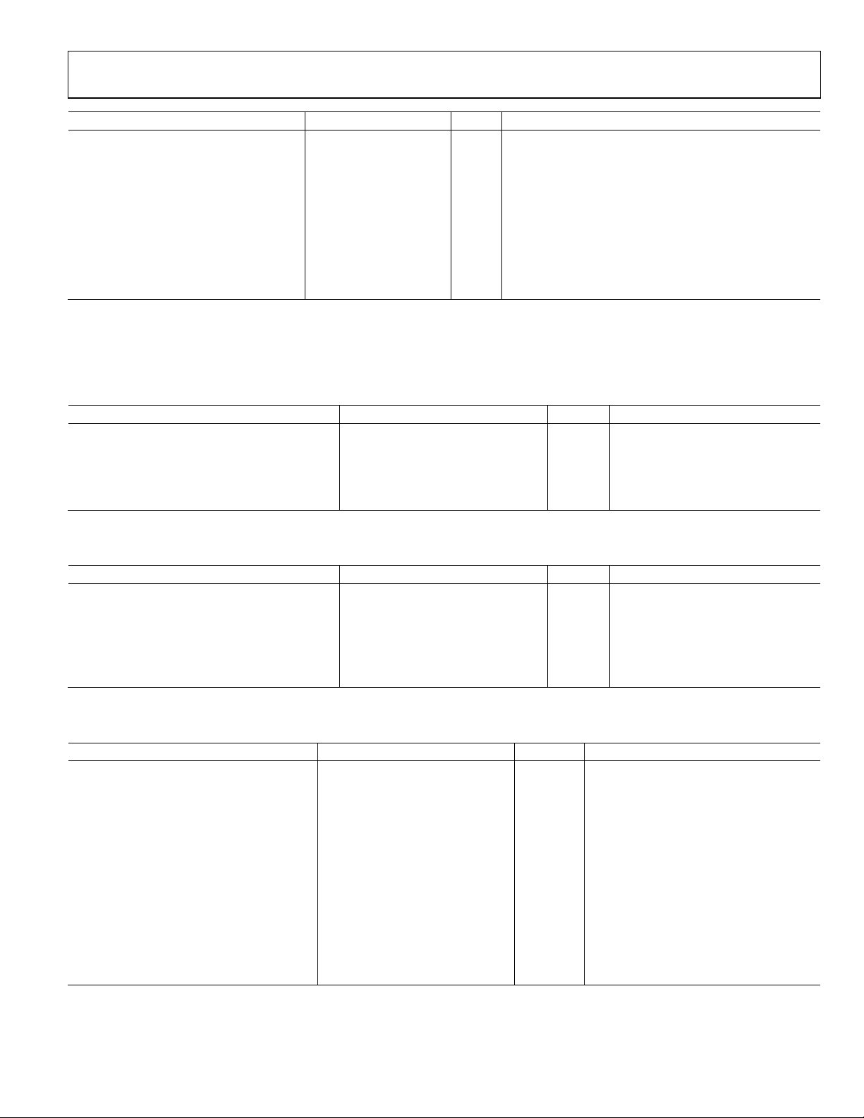
SYSTEM CLOCK INPUTS (SYSCLKP/SYSCLKN)
Table 6.
Parameter Min Typ Max Unit Test Conditions/Comments
SYSTEM CLOCK PLL BYPASSED
Input Frequency Range 500 1000 MHz
Minimum Input Slew Rate
1000
V/μs
Minimum limit imposed for jitter
performance
Duty Cycle 40 60 %
Common-Mode Voltage 1.2 V Internally generated
Differential Input Voltage Sensitivity 100 mV p-p
Minimum voltage across pins required to
ensure switching between logic states;
the instantaneous voltage on either pin
must not exceed the supply rails; can
accommodate single-ended input by ac
grounding unused input
Input Capacitance 2 pF Single-ended, each pin
Input Resistance 2.5 kΩ
Rev. G | Page 5 of 111
器件 Datasheet 文档搜索
AiEMA 数据库涵盖高达 72,405,303 个元件的数据手册,每天更新 5,000 多个 PDF 文件
