Datasheet 搜索 > ADI(亚德诺) > ADA4922-1ACPZ-R7 数据手册 > ADA4922-1ACPZ-R7 数据手册 5/19 页


¥ 0
ADA4922-1ACPZ-R7 数据手册 - ADI(亚德诺)
制造商:
ADI(亚德诺)
封装:
HVSON
Pictures:
3D模型
符号图
焊盘图
引脚图
产品图
页面导航:
导航目录
ADA4922-1ACPZ-R7数据手册
Page:
of 19 Go
若手册格式错乱,请下载阅览PDF原文件
Data Sheet ADA4922-1
Rev. A | Page 5 of 19
ABSOLUTE MAXIMUM RATINGS
Table 3.
Parameter Rating
Supply Voltage 26 V
Power Dissipation See Figure 3
Storage Temperature Range –65°C to +125°C
Operating Temperature Range –40°C to +85°C
Lead Temperature (Soldering 10 sec) 300°C
Junction Temperature 150°C
Stresses at or above those listed under Absolute Maximum
Ratings may cause permanent damage to the product. This is a
stress rating only; functional operation of the product at these
or any other conditions above those indicated in the operational
section of this specification is not implied. Operation beyond
the maximum operating conditions for extended periods may
affect product reliability.
THERMAL RESISTANCE
θ
JA
is specified for the worst-case conditions, that is, θ
JA
is
specified for a device soldered in the circuit board with its
exposed paddle soldered to a pad on the PCB surface that is
thermally connected to a copper plane, with zero airflow.
Table 4. Thermal Resistance
Package Type θ
JA
θ
JC
Unit
8-Lead SOIC with EP on 4-Layer Board 79 25
C/W
8-Lead LFCSP with EP on 4-Layer Board 81 17
C/W
MAXIMUM POWER DISSIPATION
The maximum safe power dissipation in the ADA4922-1
package is limited by the associated rise in junction temperature
(T
J
) on the die. At approximately 150°C, which is the glass
transition temperature, the plastic changes its properties. Even
temporarily exceeding this temperature limit can change the
stresses that the package exerts on the die, permanently shifting
the parametric performance of the ADA4922-1. Exceeding a
junction temperature of 150°C for an extended period can
result in changes in the silicon devices potentially causing
failure.
The power dissipated in the package (P
D
) is the sum of the
quiescent power dissipation and the power dissipated in the
package due to the load drive for all outputs. The quiescent
power is the voltage between the supply pins (V
S
) times the
quiescent current (I
S
). The power dissipated due to the load
drive depends upon the particular application. For each output,
the power due to load drive is calculated by multiplying the load
current by the associated voltage drop across the device. The
power dissipated due to all of the loads is equal to the sum of
the power dissipation due to each individual load. RMS voltages
and currents must be used in these calculations.
Airflow increases heat dissipation, effectively reducing θ
JA
. In
addition, more metal directly in contact with the package leads
from metal traces, through holes, ground, and power planes
reduces the θ
JA
. The exposed paddle on the underside of the
package must be soldered to a pad on the PCB surface that is
thermally connected to a copper plane to achieve the specified θ
JA
.
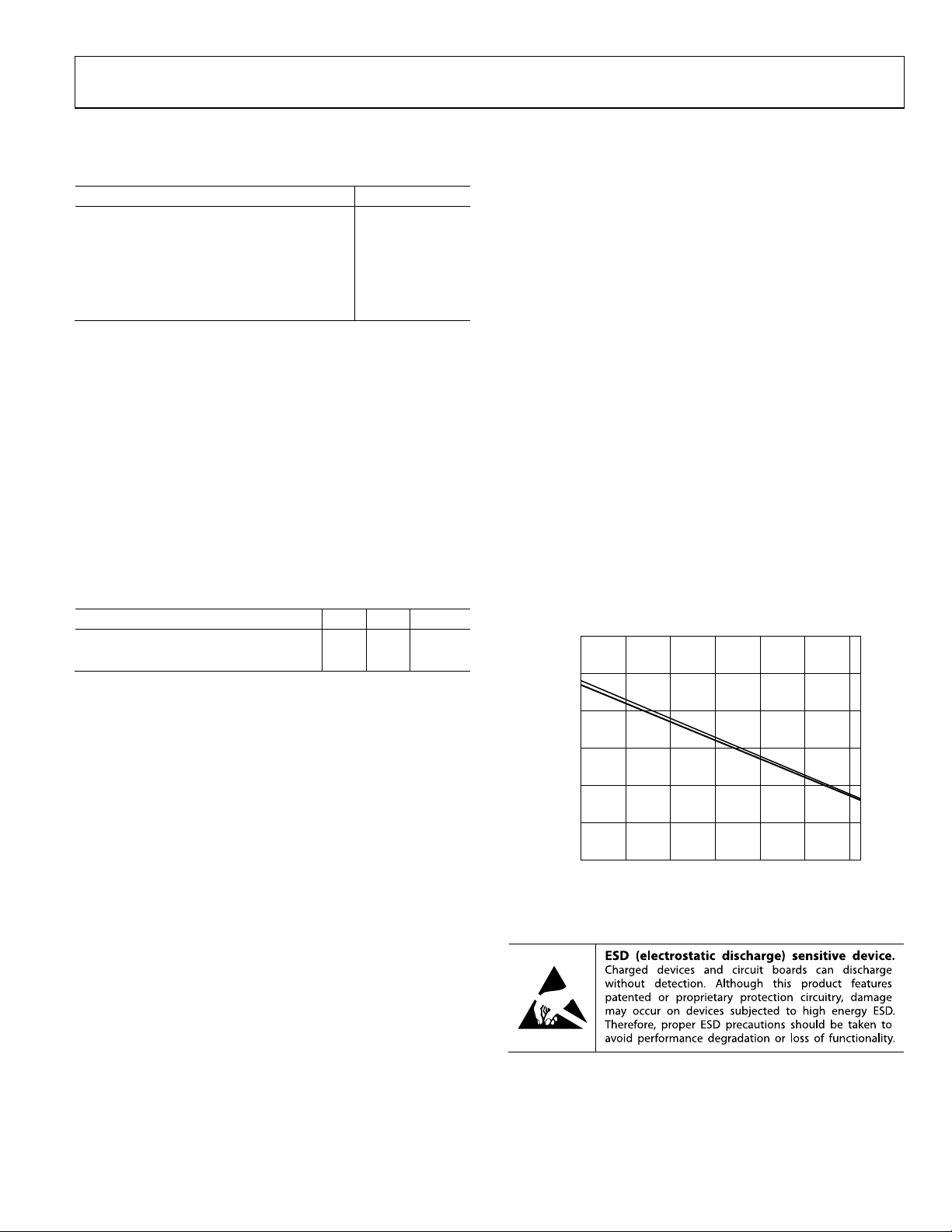
Figure 3 shows the maximum safe power dissipation in the
packages vs. the ambient temperature for the 8-lead SOIC
(79°C/W) and for the 8-lead LFCSP (81°C/W) on a JEDEC
standard 4-layer board, each with its underside paddle soldered
to a pad that is thermally connected to a PCB plane. θ
JA
values
are approximations.
3.0
0
–40 80
05681-041
AMBIENT TEMPERATURE (C)
MAXIMUM POWER DISSIPATION (W)
2.5
2.0
1.5
1.0
0.5
–20 0 20 40 60
SOIC
LFCSP
Figure 3. Maximum Power Dissipation vs. Temperature for a 4-Layer Board
ESD CAUTION
器件 Datasheet 文档搜索
AiEMA 数据库涵盖高达 72,405,303 个元件的数据手册,每天更新 5,000 多个 PDF 文件
