Datasheet 搜索 > 电源监控芯片 > ADI(亚德诺) > ADM1166ASUZ-REEL 数据手册 > ADM1166ASUZ-REEL 数据手册 6/33 页
 器件3D模型
¥ 146.495
ADM1166ASUZ-REEL 数据手册 - ADI(亚德诺)
制造商:
ADI(亚德诺)
分类:
电源监控芯片
封装:
TQFP-48
描述:
超序与余量控制和非易失故障记录 Super Sequencer with Margining Control and Nonvolatile Fault Recording
Pictures:
3D模型
符号图
焊盘图
引脚图
产品图
页面导航:
导航目录
ADM1166ASUZ-REEL数据手册
Page:
of 33 Go
若手册格式错乱,请下载阅览PDF原文件
ADM1166 Data Sheet
Rev. A | Page 6 of 33
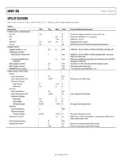
Parameter Min Typ Max Unit Test Conditions/Comments
Standard (Digital Output) Mode
(PDO1 to PDO10)
V
OH
2.4 V V
PU
(pull-up to VDDCAP or VPx) = 2.7 V, I
OH
= 0.5 mA
4.5 V V
PU
to VPx = 6.0 V, I
OH
= 0 mA
V
PU
− 0.3 V V
PU
≤ 2.7 V, I
OH
= 0.5 mA
V
OL
0 0.50 V I
OL
= 20 mA
I
OL
2
20 mA Maximum sink current per PDOx pin
I
SINK
2
60 mA Maximum total sink for all PDOx pins
R
PULL-UP
16 20 29 kΩ Internal pull-up
I
SOURCE
(VPx)
2
2 mA
Current load on any VPx pull-ups, that is, total source
current available through any number of PDO pull-up
switches configured onto any one VPx pin
Three-State Output Leakage
Current
10 μA V
PDO
= 14.4 V
Oscillator Frequency 90 100 110 kHz All on-chip time delays derived from this clock
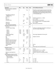
DIGITAL INPUTS (VXx, A0, A1)
Input High Voltage, V
IH
2.0 V Maximum V
IN
= 5.5 V
Input Low Voltage, V
IL
0.8 V Maximum V
IN
= 5.5 V
Input High Current, I
IH
−1 μA V
IN
= 5.5 V
Input Low Current, I
IL
1 μA V
IN
= 0 V
Input Capacitance 5 pF
Programmable Pull-Down Current,
I
PULL-DOWN
20 μA VDDCAP = 4.75 V, T
A
= 25°C, if known logic state is required
SERIAL BUS DIGITAL INPUTS (SDA, SCL)
Input High Voltage, V
IH
2.0 V
Input Low Voltage, V
IL
0.8 V
Output Low Voltage, V
OL
2
0.4 V I
OUT
= −3.0 mA
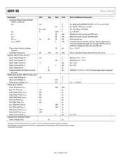
SERIAL BUS TIMING
3
Clock Frequency, f
SCLK
400 kHz
Bus Free Time, t
BUF
1.3 μs
Start Setup Time, t
SU;STA
0.6 μs
Stop Setup Time, t
SU;STO
0.6 μs
Start Hold Time, t
HD;STA
0.6 μs
SCL Low Time, t
LOW
1.3 μs
SCL High Time, t
HIGH
0.6 μs
SCL, SDA Rise Time, t
R
300 ns
SCL, SDA Fall Time, t
F
300 ns
Data Setup Time, t
SU;DAT
100 ns
Data Hold Time, t
HD;DAT
250 ns
Input Low Current, I
IL
1 μA V
IN
= 0 V
SEQUENCING ENGINE TIMING
State Change Time 10 μs
1
At least one of the VH and VPx pins must be ≥ 3.0 V to maintain the device supply on VDDCAP.
2
Specification is not production tested but is supported by characterization data at initial product release.
3
Guaranteed by design.
器件 Datasheet 文档搜索
AiEMA 数据库涵盖高达 72,405,303 个元件的数据手册,每天更新 5,000 多个 PDF 文件
