Datasheet 搜索 > 开发套件 > TI(德州仪器) > ADS4449EVM 数据手册 > ADS4449EVM 数据手册 41/56 页

¥ 5221.148
ADS4449EVM 数据手册 - TI(德州仪器)
制造商:
TI(德州仪器)
分类:
开发套件
Pictures:
3D模型
符号图
焊盘图
引脚图
产品图
页面导航:
引脚图在P3P4Hot
典型应用电路图在P41P42P43P44
原理图在P21
封装尺寸在P51P53P54
标记信息在P51
封装信息在P50P51P52P53P54
技术参数、封装参数在P5
应用领域在P1P56
电气规格在P7P8
导航目录
ADS4449EVM数据手册
Page:
of 56 Go
若手册格式错乱,请下载阅览PDF原文件
0.1
0.2
0.3
0.4
0.5
0.6
0.7
0.8
0.9
1
100 200 300 400 500
Frequency (MHz)
Differential Input Resistance, Rin (kΩ)
G037
0
1
2
3
4
5
6
100 200 300 400 500
Frequency (MHz)
Differential Input Capacitance, Cin (pF)
G038
XINP
(1)
XINM
(1)
R
IN
Z
IN
(2)
C
IN
41
ADS4449
www.ti.com
SBAS603A –APRIL 2013–REVISED JANUARY 2016
Product Folder Links: ADS4449
Submit Documentation FeedbackCopyright © 2013–2016, Texas Instruments Incorporated
9 Application and Implementation
NOTE
Information in the following applications sections is not part of the TI component
specification, and TI does not warrant its accuracy or completeness. TI’s customers are
responsible for determining suitability of components for their purposes. Customers should
validate and test their design implementation to confirm system functionality.
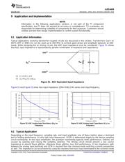
9.1 Application Information
Typical applications involving transformer-coupled circuits are discussed in this section. Transformers (such as
ADT1-1WT or WBC1-1) can be used up to 250 MHz to achieve good phase and amplitude balances at ADC
inputs. While designing the dc driving circuits, the ADC input impedance must be considered. Figure 51 shows
that ADC input impedance is represented by parallel combination of resistance and capacitance.
(1) X = A, B, C, or D.
(2) Z
IN
= R
IN
|| (1 / jωC
IN
).
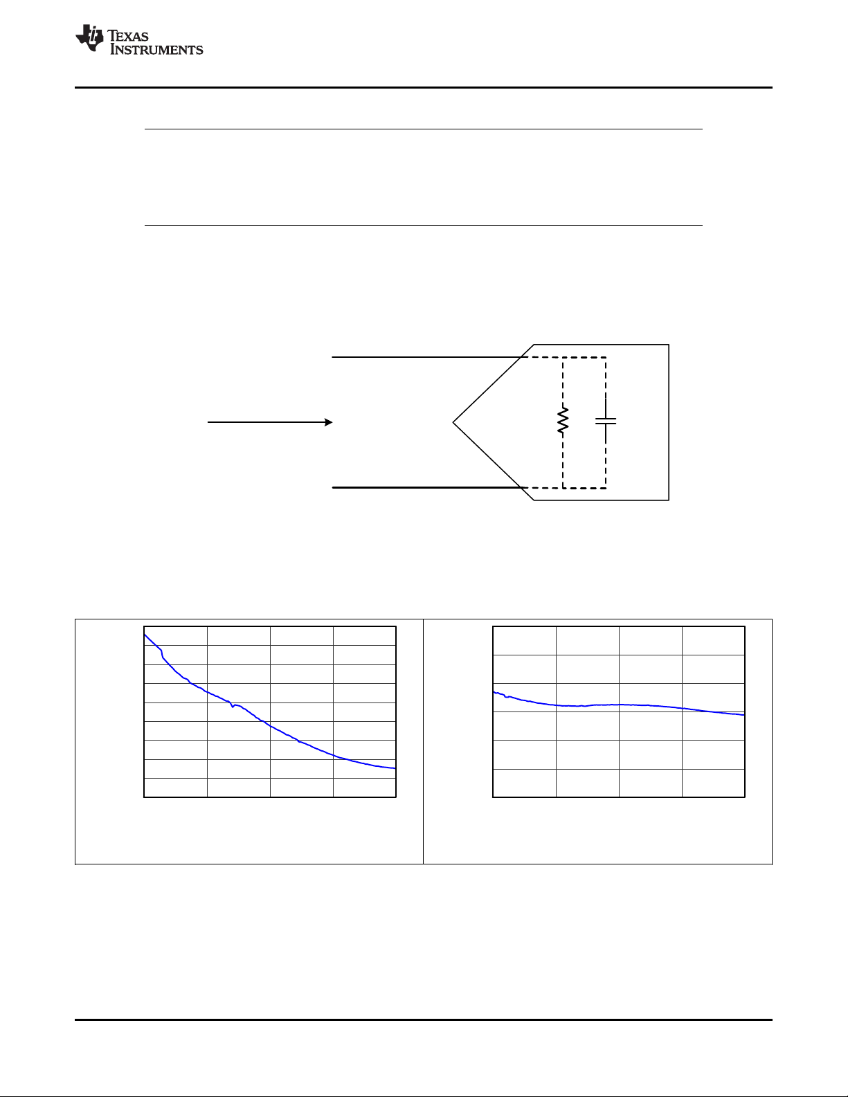
Figure 51. ADC Equivalent Input Impedance
Figure 52 and Figure 53 show how input impedance (ZIN= RIN|| CIN) varies over input frequency.
Figure 52. ADC Analog Input Resistance (R
IN
) vs
Frequency
Figure 53. ADC Analog Input Capacitance (C
IN
) vs
Frequency
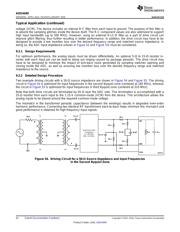
9.2 Typical Application
Depending on the input frequency, sampling rate, and input amplitude, one of these metrics plays a dominant
part in limiting performance. At very high input frequencies, SFDR is determined largely by the device sampling
circuit nonlinearity. At low input amplitudes, the quantizer nonlinearity typically limits performance. Glitches are
caused by opening and closing the sampling switches. The driving circuit should present a low source
impedance to absorb these glitches, otherwise these glitches may limit performance. A low impedance path
between the analog input terminals and VCM is required from the common-mode switching currents perspective
as well. This impedance can be achieved by using two resistors from each input terminated to the common-mode
器件 Datasheet 文档搜索
AiEMA 数据库涵盖高达 72,405,303 个元件的数据手册,每天更新 5,000 多个 PDF 文件
