Datasheet 搜索 > 开发套件 > TI(德州仪器) > ADS4449EVM 数据手册 > ADS4449EVM 数据手册 42/56 页

¥ 5221.148
ADS4449EVM 数据手册 - TI(德州仪器)
制造商:
TI(德州仪器)
分类:
开发套件
Pictures:
3D模型
符号图
焊盘图
引脚图
产品图
页面导航:
引脚图在P3P4Hot
典型应用电路图在P41P42P43P44
原理图在P21
封装尺寸在P51P53P54
标记信息在P51
封装信息在P50P51P52P53P54
技术参数、封装参数在P5
应用领域在P1P56
电气规格在P7P8

导航目录
ADS4449EVM数据手册
Page:
of 56 Go
若手册格式错乱,请下载阅览PDF原文件
VCM
Device
0.1 PF
25 :
25 :
10 :
10 :
10 pF
82 nH
25 :
25 :
INP
INM
R
IN
C
IN
1:1
50 :
1:1
Band-Pass Filter
Centered at
f
0
= 185 MHz
BW = 125 MHz
T1
T2
0.1 PF
0.1 PF
42
ADS4449
SBAS603A –APRIL 2013–REVISED JANUARY 2016
www.ti.com
Product Folder Links: ADS4449
Submit Documentation Feedback Copyright © 2013–2016, Texas Instruments Incorporated
Typical Application (continued)
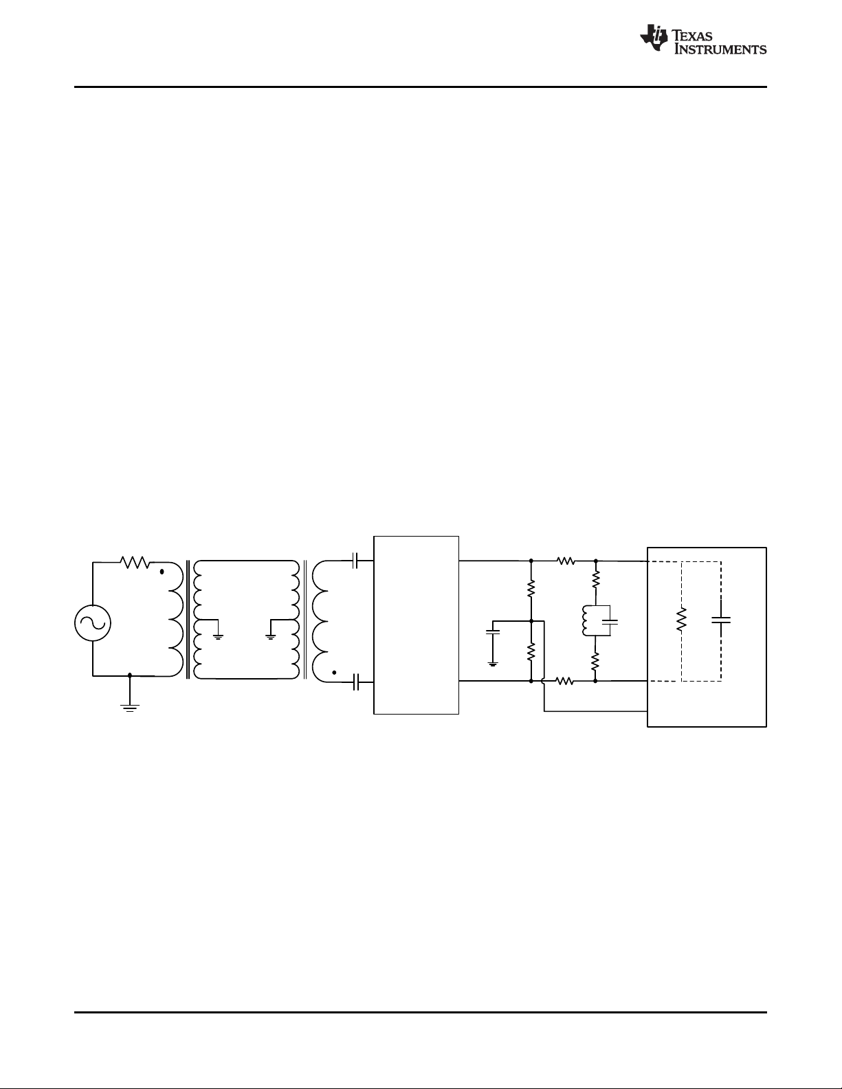
voltage (VCM). The device includes an internal R-C filter from each input to ground. The purpose of this filter is
to absorb the sampling glitches inside the device itself. The R-C component values are also optimized to support
high input bandwidth (up to 500 MHz). However, using an external R-LC-R filter as a part of drive circuit can
improve glitch filtering, thus further resulting in better performance. In addition, the drive circuit may have to be
designed to provide a low insertion loss over the desired frequency range and matched source impedance. In
doing so, the ADC input impedance (shown in Figure 52 and Figure 53) must be considered.
9.2.1 Design Requirements
For optimum performance, the analog inputs must be driven differentially. An optional 5-Ω to 15-Ω resistor in-
series with each input pin can be kept to damp out ringing caused by package parasitic. The drive circuit may
have to be designed to minimize the impact of kick-back noise generated by sampling switches opening and
closing inside the ADC, as well as ensuring low insertion loss over the desired frequency range and matched
impedance to the source.
9.2.2 Detailed Design Procedure
Two example driving circuits with a 50-Ω source impedance are shown in Figure 54 and Figure 55. The driving
circuit in Figure 54 is optimized for input frequencies in the second Nyquist zone (centered at 185 MHz), whereas
the circuit in Figure 55 is optimized for input frequencies in third Nyquist zone (centered at 310 MHz).
Note that both drive circuits are terminated by 50 Ω near the ADC side. This termination is accomplished with a
25-Ω resistor from each input to the 1.15-V common-mode (VCM) from the device. This architecture allows the
analog inputs to be biased around the required common-mode voltage.
The mismatch in the transformer parasitic capacitance (between the windings) results in degraded even-order
harmonic performance. Connecting two identical RF transformers back-to-back helps minimize this mismatch and
good performance is obtained for high-frequency input signals.
Figure 54. Driving Circuit for a 50-Ω Source Impedance and Input Frequencies
in the Second Nyquist Zone
器件 Datasheet 文档搜索
AiEMA 数据库涵盖高达 72,405,303 个元件的数据手册,每天更新 5,000 多个 PDF 文件
