Datasheet 搜索 > 开发套件 > TI(德州仪器) > ADS4449EVM 数据手册 > ADS4449EVM 数据手册 44/56 页

¥ 5221.148
ADS4449EVM 数据手册 - TI(德州仪器)
制造商:
TI(德州仪器)
分类:
开发套件
Pictures:
3D模型
符号图
焊盘图
引脚图
产品图
页面导航:
引脚图在P3P4Hot
典型应用电路图在P41P42P43P44
原理图在P21
封装尺寸在P51P53P54
标记信息在P51
封装信息在P50P51P52P53P54
技术参数、封装参数在P5
应用领域在P1P56
电气规格在P7P8
导航目录
ADS4449EVM数据手册
Page:
of 56 Go
若手册格式错乱,请下载阅览PDF原文件
−120
−100
−80
−60
−40
−20
0
0 25 50 75 100 125
Frequency (MHz)
Amplitude (dB)
G005
−120
−100
−80
−60
−40
−20
0
0 25 50 75 100 125
Frequency (MHz)
Amplitude (dB)
G006
44
ADS4449
SBAS603A –APRIL 2013–REVISED JANUARY 2016
www.ti.com
Product Folder Links: ADS4449
Submit Documentation Feedback Copyright © 2013–2016, Texas Instruments Incorporated
Typical Application (continued)
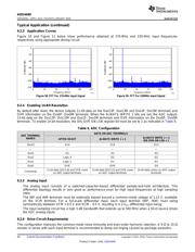
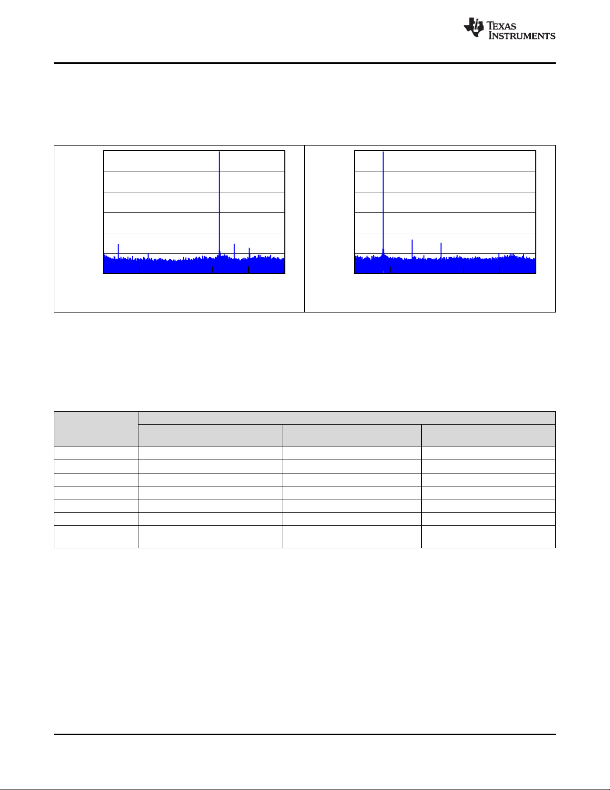
9.2.3 Application Curves
Figure 10 and Figure 11 below show performance obtained at 170-MHz and 230-MHz input frequencies
respectively using appropriate driving circuit.
Figure 58. FFT For 170-MHz Input Signal Figure 59. FFT For 230MHz Input Signal
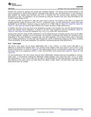
9.2.4 Enabling 14-Bit Resolution
By default after reset, the device outputs 11-bit data on the Dxx13P, Dxx13M and Dxx3P, Dxx3M terminals and
OVR information on the Dxx0P, Dxx0M terminals. When the ALWAYS WRITE 1 bits are set, the ADC outputs
13-bit data on the Dxx13P, Dxx13M and Dxx1P, Dxx1M terminals and OVR information on the Dxx0P, Dxx0M
terminals. To enable 14-bit resolution, the DIS OVR ON LSB register bit must be set to 1 as indicated in Table 6.
Table 6. ADC Configuration
ADC TERMINAL
NAMES
DATA ON ADC TERMINALS
AFTER RESET ALWAYS WRITE 1 = 1
ALWAYS WRITE 1 = 1
DIS OVR ON LSB = 1
Dxx13 D13 D13 D13
— — — —
Dxx3 D3 D3 D3
Dxx2 Logic 0 D2 D2
Dxx1 Logic 1 D1 D1
Dxx0 OVR OVR D0
Comments
11-bit data (D[13:3]) and OVR come
on ADC output terminals
13-bit data (D[13:1]) and OVR come
on ADC output terminals
14-bit data comes on ADC output
terminals
9.2.5 Analog Input
The analog input consists of a switched-capacitor-based differential sample-and-hold architecture. This
differential topology results in very good ac performance even for high input frequencies at high sampling
rates.
The INP and INM terminals must be externally biased around a common-mode voltage of 1.15 V, available
on the VCM terminal. For a full-scale differential input, each input terminal (INP, INM) must swing
symmetrically between VCM + 0.5 V and VCM – 0.5 V, resulting in a 2-V
PP
differential input swing.
The input sampling circuit has a high 3-dB bandwidth that extends up to 500 MHz when a 50-Ω source drives
the ADC analog inputs.
9.2.6 Drive Circuit Requirements
This configuration improves the common-mode noise immunity and even-order harmonic rejection. A 5-Ω to 15-Ω
resistor in series with each input terminal is recommended to damp out ringing caused by package parasitics.
器件 Datasheet 文档搜索
AiEMA 数据库涵盖高达 72,405,303 个元件的数据手册,每天更新 5,000 多个 PDF 文件
