Datasheet 搜索 > AD转换器 > TI(德州仪器) > ADS5547IRGZRG4 数据手册 > ADS5547IRGZRG4 数据手册 25/57 页
 器件3D模型
¥ 0
ADS5547IRGZRG4 数据手册 - TI(德州仪器)
制造商:
TI(德州仪器)
分类:
AD转换器
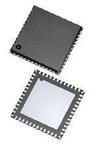
封装:
QFN-48
描述:
14 - BIT , 210 MSPS的DDR LVDS / CMOS输出的ADC 14-BIT, 210 MSPS ADC WITH DDR LVDS/CMOS OUTPUTS
Pictures:
3D模型
符号图
焊盘图
引脚图
产品图
页面导航:
引脚图在P12P22P23P24P25Hot
封装尺寸在P50P52P53
型号编码规则在P2
标记信息在P2P50
封装信息在P2P50P51P52P53
技术参数、封装参数在P3P46P47P48
应用领域在P1P57
电气规格在P4P5P6
型号编号列表在P1
导航目录
ADS5547IRGZRG4数据手册
Page:
of 57 Go
若手册格式错乱,请下载阅览PDF原文件
www.ti.com
ADS5547
SLWS192A – NOVEMBER 2006 – REVISED MAY 2007
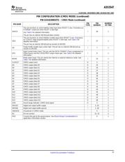
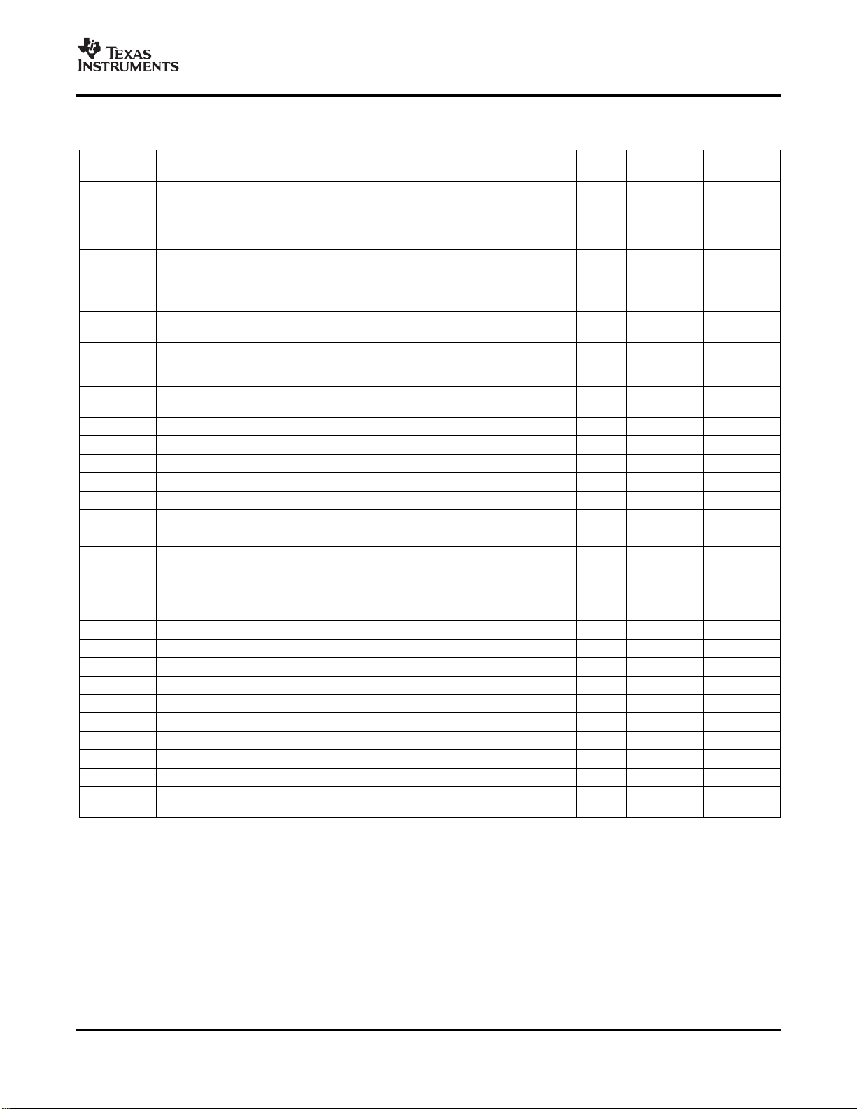
PIN CONFIGURATION (CMOS MODE) (continued)
PIN ASSIGNMENTS – CMOS Mode (continued)
PIN PIN NUMBER
PIN NAME DESCRIPTION
TYPE NUMBER OF PINS
This pin functions as serial interface data input when RESET is low. It functions as
STANDBY control pin when RESET is tied high.
SDATA I 28 1
See Table 4 for detailed information.
The pin has an internal 100 k Ω pull-down resistor.
This pin functions as serial interface enable input when RESET is low. It functions
as CLKOUT edge programmability when RESET is tied high. See Table 5 for
SEN I 27 1
detailed information.
The pin has an internal 100-k Ω pull-up resistor to DRVDD.
Output buffer enable input, active high. The pin has an internal 100-k Ω pull-up
OE I 7 1
resistor to DRVDD.
Data Format Select input. This pin sets the DATA FORMAT (Twos complement or
DFS Offset binary) and the LVDS/CMOS output mode type. See Table 6 for detailed I 6 1
information.
Mode select input. This pin selects the internal or external reference mode. See
MODE I 23 1
Table 7 for detailed information.
CLKOUT CMOS output clock O 5 1
D0 CMOS output data D0 O 33 1
D0 CMOS output data D1 O 34 1
D2 CMOS output data D2 O 37 1
D2 CMOS output data D3 O 38 1
D4 CMOS output data D4 O 39 1
D4 CMOS output data D5 O 40 1
D6 CMOS output data D6 O 41 1
D7 CMOS output data D7 O 42 1
D8 CMOS output data D8 O 43 1
D9 CMOS output data D9 O 44 1
D10 CMOS output data D10 O 45 1
D11 CMOS output data D11 O 46 1
D12 CMOS output data D12 O 47 1
D13 CMOS output data D13 O 48 1
OVR Out-of-range indicator, CMOS level signal O 3 1
DRVDD Digital and output buffer supply I 2, 35 2
DRGND Digital and output buffer ground I 1, 36 2
UNUSED Unused pin in CMOS mode 4 1
NC Do not connect 31, 32 2
PAD Connect the pad to the ground plane. See Board Design Considerations in 0 1
application information section.
25
Submit Documentation Feedback
器件 Datasheet 文档搜索
AiEMA 数据库涵盖高达 72,405,303 个元件的数据手册,每天更新 5,000 多个 PDF 文件
