Datasheet 搜索 > 微控制器 > ADI(亚德诺) > ADUC7021BCPZ62-RL7 数据手册 > ADUC7021BCPZ62-RL7 数据手册 4/104 页
 器件3D模型
¥ 39.428
ADUC7021BCPZ62-RL7 数据手册 - ADI(亚德诺)
制造商:
ADI(亚德诺)
分类:
微控制器
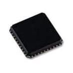
封装:
LFCSP-40
描述:
精密模拟微控制器, 12位模拟I / O , ARM7TDMI MCU Precision Analog Microcontroller, 12-Bit Analog I/O, ARM7TDMI MCU
Pictures:
3D模型
符号图
焊盘图
引脚图
产品图
页面导航:
引脚图在P21P22P23P25P26P28P31P33P68P97P98Hot
原理图在P1P9P85P86P87P88
封装尺寸在P97
焊盘布局在P94
型号编码规则在P1P4P9P47P96P101
焊接温度在P20
功能描述在P4P21P23P26P28P31P33P68P97P98
技术参数、封装参数在P1P10P13P20P38P50
应用领域在P1
电气规格在P35
导航目录
ADUC7021BCPZ62-RL7数据手册
Page:
of 104 Go
若手册格式错乱,请下载阅览PDF原文件
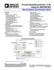
ADuC7019/20/21/22/24/25/26/27/28/29 Data Sheet
Rev. F | Page 4 of 104
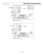
GENERAL DESCRIPTION
The ADuC7019/20/21/22/24/25/26/27/28/29 are fully integrated,
1 MSPS, 12-bit data acquisition systems incorporating high
performance multichannel ADCs, 16-bit/32-bit MCUs, and
Flash®/EE memory on a single chip.
The ADC consists of up to 12 single-ended inputs. An additional
four inputs are available but are multiplexed with the four DAC
output pins. The four DAC outputs are available only on certain
models (ADuC7020, ADuC7026, ADuC7028, and ADuC7029).
However, in many cases where the DAC outputs are not present,
these pins can still be used as additional ADC inputs, giving a
maximum of 16 ADC input channels. The ADC can operate in
single-ended or differential input mode. The ADC input voltage
is 0 V to V
REF
. A low drift band gap reference, temperature sensor,
and voltage comparator complete the ADC peripheral set.
Depending on the part model, up to four buffered voltage
output DACs are available on-chip. The DAC output range is
programmable to one of three voltage ranges.
The devices operate from an on-chip oscillator and a PLL
generating an internal high frequency clock of 41.78 MHz
(UCLK). This clock is routed through a programmable clock
divider from which the MCU core clock operating frequency
is generated. The microcontroller core is an ARM7TDMI®,
16-bit/32-bit RISC machine, which offers up to 41 MIPS peak
performance. Eight kilobytes of SRAM and 62 kilobytes of
nonvolatile Flash/EE memory are provided on-chip. The
ARM7TDMI core views all memory and registers as a single
linear array.
On-chip factory firmware supports in-circuit serial download
via the UART or I
2
C serial interface port; nonintrusive emulation
is also supported via the JTAG interface. These features are
incorporated into a low cost QuickStart™ development system
supporting this MicroConverter® family.
The parts operate from 2.7 V to 3.6 V and are specified over an
industrial temperature range of −40°C to +125°C. When
operating at 41.78 MHz, the power dissipation is typically
120 mW. The ADuC7019/20/21/22/24/25/26/27/28/29 are
available in a variety of memory models and packages (see
Ordering Guide).
1MSPS
12-BIT ADC
DAC0
12-BIT
DAC
DAC1
DAC2
DAC3
3-PHASE
PWM
(SEE NOTE 1)
ADuC7020
XCLKI
XCLKO
RST
V
REF
MUX
TEMP
SENSOR
BAND GAP
REF
OSC
AND PLL
PSM
POR
CMP0
CMP1
CMP
OUT
PLA
4 GENERAL-
PURPOSE TIMERS
2k × 32 SRAM
31k × 16 FLASH/EEPROM
SERIAL I/O
UART, SPI, I
2
C
GPIO
JTAG
ARM7TDMI-BASED MCU WITH
ADDITIONAL PERIPHERALS
12-BIT
DAC
12-BIT
DAC
12-BIT
DAC
NOTES
1. SEE APPLICATION NOTE AN-798.
04955-101
ADC0 TO ADC4,
ADC12 TO ADC15
Figure 2.
器件 Datasheet 文档搜索
AiEMA 数据库涵盖高达 72,405,303 个元件的数据手册,每天更新 5,000 多个 PDF 文件
